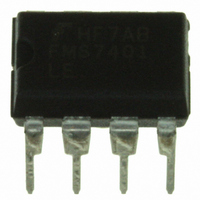
FMS7401LEN Fairchild Semiconductor, FMS7401LEN Datasheet - Page 26

FMS7401LEN
Manufacturer Part Number
FMS7401LEN
Description
IC CTRLR POWER DGTL EEPROM 8DIP
Manufacturer
Fairchild Semiconductor
Datasheet
1.FMS7401LVN.pdf
(81 pages)
Specifications of FMS7401LEN
Applications
Digital Power Controller
Core Processor
8-Bit
Program Memory Type
EEPROM (1 kB)
Ram Size
64 x 8
Number Of I /o
6
Voltage - Supply
2.7 V ~ 3.6 V
Operating Temperature
-40°C ~ 85°C
Mounting Type
Through Hole
Package / Case
8-DIP (0.300", 7.62mm)
Mounting Style
Through Hole
Lead Free Status / RoHS Status
Lead free / RoHS Compliant
Interface
-
Controller Series
-
Lead Free Status / Rohs Status
Lead free / RoHS Compliant
Other names
FMS7401LEN_NL
FMS7401LEN_NL
FMS7401LEN_NL
Available stocks
Company
Part Number
Manufacturer
Quantity
Price
Company:
Part Number:
FMS7401LEN14
Manufacturer:
Rohm
Quantity:
21 626
FMS7401L
Bits 7-2 (CL[5:0]) is the comparator voltage threshold level selection bits of the Comparator Control (COMP) register. The CL
bits may be programmed to select one of the voltage threshold levels as the inverting input of the analog comparator. Refer to
Table 9
Bit 1 of the Comparator Control (COMP) register is the Programmable Comparator circuit’s voltage loop (VLOOP) configura-
tion enable bit. If VLOOP=0, the Programmable Comparator circuit is configured to compare the analog G4/AIN0 or G2/AIN2
input (COMPSEL=0 or 1) to one of the 63 voltage threshold levels. If VLOOP=1, enables the voltage loop configuration where
the analog G4/AIN0 or G2/AIN2 input (COMPSEL=0 or 1) to the Uncommitted (Error) Amplifier output (A
Bit 7 of the Digital Delay (DDELAY) register is the Programmable Comparator circuit enable (COMPEN) bit. If COMPEN=0,
the Programmable Comparator circuit is disabled and the C
circuit is enabled and the C
The comparator output (C
ator Control (COMP) register. Software may only read the COUT bit to monitor the comparator’s activity. The COUT bit
cannot cause a microcontroller hardware interrupt or perform any other action.
26
G
G 4 /
2
/
A
A
I N
I N
2
0
and
Table 10
C
L
7
[ 5 ]
for a detailed list of voltages.
C
L
6
[
4
OUT
]
OUT
A
Figure 8. Programmable Comparator Block Diagram (VLOOP = 0)
C
A D
d
) signal is latched by the main system instruction (F
j u
O
C
C
signal generated by the comparison of the two inputs.
s t R e
M
N
L
5
T
[ 3 ]
P
R
S E L
L
2 [ 6 ]
f
e r e
n c
C
e
L
4
V
[ 2 ]
o l
t
A
a
C
g e
H
5
C
L
3
[ 1 ]
C
L
2
[ 0 ]
OUT
signal is low. If COMPEN=1, the Programmable Comparator
V
L
O O P
1
F
C
R
C
O
E
0
L
U T
P
K 2
ICLK
5
W
M
+
_
C
) clock into bit 0 (COUT) of the Compar-
E
o
D D
n
m p
3
C
[ 3 ]
(
o
a
C
m p
D D E L A Y
r
R e g i s t e r
D
O
a
D D
I G I
t
M
o
a
r
r
P
C
2
a
T
[ 2 ]
)
I
t
A L D E L A Y
R
o
R e g i s t e r
r
C
C
D D
U
o n
I
1
T
[ 1 ]
t r
PRODUCT SPECIFICATION
o l
D D
0
[ 0 ]
REV. 1.0.3 1/24/05
OUT
P
W
M
).
O
F F
(
C O
W K
U T
E
N
[ 6 ]
)


