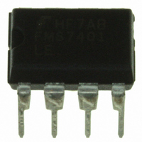
FMS7401LEN Fairchild Semiconductor, FMS7401LEN Datasheet - Page 60

FMS7401LEN
Manufacturer Part Number
FMS7401LEN
Description
IC CTRLR POWER DGTL EEPROM 8DIP
Manufacturer
Fairchild Semiconductor
Datasheet
1.FMS7401LVN.pdf
(81 pages)
Specifications of FMS7401LEN
Applications
Digital Power Controller
Core Processor
8-Bit
Program Memory Type
EEPROM (1 kB)
Ram Size
64 x 8
Number Of I /o
6
Voltage - Supply
2.7 V ~ 3.6 V
Operating Temperature
-40°C ~ 85°C
Mounting Type
Through Hole
Package / Case
8-DIP (0.300", 7.62mm)
Mounting Style
Through Hole
Lead Free Status / RoHS Status
Lead free / RoHS Compliant
Interface
-
Controller Series
-
Lead Free Status / Rohs Status
Lead free / RoHS Compliant
Other names
FMS7401LEN_NL
FMS7401LEN_NL
FMS7401LEN_NL
Available stocks
Company
Part Number
Manufacturer
Quantity
Price
Company:
Part Number:
FMS7401LEN14
Manufacturer:
Rohm
Quantity:
21 626
PRODUCT SPECIFICATION
FMS7401L
The opcode must be shifted in after Vcc settles to its nominal voltage level and before the system reset sequence (T
) com-
RESET
pletes. Otherwise, the device will begin with its normal operation executing the instruction program residing in the code
EEPROM memory. If an external reset is applied by bringing the RESET pin low, the 10-bit opcode may be shifted once
RESET is released and before the system reset sequence completes.
12.2 Programming Protocol
Once the device is in programming mode, the programming protocol and commands may be issued. An externally controlled
4-wire interface consisting of a LOAD (G3) control, serial data SHIFT_IN (G4) input, serial data SHIFT_OUT (G2) output,
and CLOCK (G1) pins are used to access the internal memory and registers. Communication between the external programmer
and the FMS7401L is performed through a 32-bit command and response word, as described in
Table
23. The serial data tim-
ing for the 4-wire interface is shown in
Figure 20
and the programming protocol is shown in
Figure
19. In order to exit pro-
gramming mode, the device must be powered down or an external reset must be applied.
12.2.1 Byte Write Sequence
After the external programmer puts the FMS7401L into programming mode, the LOAD pin must be set to Vcc before serially
shifting the first 32-bit command word using the SHIFT_IN and CLOCK signals. By definition, bit 31 of the command word
must be shifted first followed by all other bits. With each bit of the 32-bit write command word shifted, the device shifts out a
bit of the 32-bit response word from the previous command through the SHIFT_OUT pin. The external programmer may sam-
ple SHIFT_OUT after T
from the rising edge of CLOCK. The serial response word sent immediately after entering pro-
ACCESS
gramming mode may contain indeterminate data.
After all 32 bits of the command word are shifted, the external programmer must set the LOAD signal to 0V and apply two
clock pulses to the CLOCK signal, as shown in
Figure
19, to complete the program cycle. Once the LOAD signal is brought
low, the SHIFT_OUT pin acts as the handshaking signal between the device and external programmer hardware. When execut-
ing the write command, the device sets SHIFT_OUT low by the time the external programmer has issued the second rising
edge of CLOCK informing the external programmer that the memory write is in progress. The external programmer must wait
T
for SHIFT_OUT to return high before returning the LOAD signal to Vcc to initiate the next command cycle.
READY
12.2.2 Page Write Sequence
Page mode is a convenient and fast way to program the code EEPROM memory. In this mode, 16 bytes of data are written
using a single write command followed by a stream of data bytes. Only full pages can be written in page mode where the
4
address in the command word points to the beginning of a page.
After all 16 bytes of data has been shifted, the data will be
written at once speeding up the total write time by a factor of 16 compared to byte mode programming.
Figure 21
shows the
page mode programming protocol.
Page mode’s 32-bit write command word is similar to a byte write command except that bit 31 must be set to 1 in order to
enable page mode. The address in the page-write command word (bits 17 to 8) must select the page to program the 16 bytes of
data (the page address is a multiple of the page size: 0x000, 0x010, 0x020, etc.). The first byte of the page to program must be
placed in the last 8 bits of the page-write command word (bits 7 to 0). All other bytes in the page must immediately follow after
the initial page-write command has been entered.
The LOAD pin must be set to Vcc before serially shifting in the 32-bit page-write command word using the SHIFT_IN and
CLOCK signals. By definition, bit 31 of the command word must be shifted first followed by all other bits. After all 32 bits of
the command word are shifted, the external programmer must set the LOAD signal to 0V and apply two clock pulses to the
CLOCK signal to latch the first byte of the page in its temporary data buffer. The LOAD signal must be returned to Vcc in
order for the external programmer to shift the second byte of the page into the device (without repeating the command word).
Once all 8 bits of the byte are shifted, the LOAD signal must again be set to 0V followed by two clocks pulses of the CLOCK
signal in order to latch byte into its temporary data buffer. This process must be repeated until all 16 bytes are loaded into their
data buffers.
th
While the 16
byte of data is being latched, the actual write to the code EEPROM page, selected by the address in the 32-bit
page-write command word, occurs. Once the LOAD signal is brought low, the SHIFT_OUT pin acts as the handshaking signal
60
REV. 1.0.3 1/24/05


