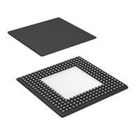
CYP15G0401RB-BGXC Cypress Semiconductor Corp, CYP15G0401RB-BGXC Datasheet - Page 10

CYP15G0401RB-BGXC
Manufacturer Part Number
CYP15G0401RB-BGXC
Description
IC RECEIVER HOTLINK 256LBGA
Manufacturer
Cypress Semiconductor Corp
Series
HOTlink II™r
Type
Transceiverr
Datasheet
1.CYP15G0401RB-BGXC.pdf
(35 pages)
Specifications of CYP15G0401RB-BGXC
Package / Case
256-LBGA Exposed Pad, 32-HLBGA
Number Of Drivers/receivers
0/4
Protocol
Multiprotocol
Voltage - Supply
3.135 V ~ 3.465 V
Mounting Type
Surface Mount
Product
PHY
Data Rate
1500 MBd
Supply Voltage (max)
3.465 V
Supply Voltage (min)
3.135 V
Supply Current
0.69 A
Maximum Operating Temperature
+ 70 C
Minimum Operating Temperature
0 C
Mounting Style
SMD/SMT
Number Of Channels
4RX
Lead Free Status / RoHS Status
Lead free / RoHS Compliant
Lead Free Status / RoHS Status
Lead free / RoHS Compliant, Lead free / RoHS Compliant
Available stocks
Company
Part Number
Manufacturer
Quantity
Price
Company:
Part Number:
CYP15G0401RB-BGXC
Manufacturer:
Cypress Semiconductor Corp
Quantity:
10 000
Document #: 38-02111 Rev. **
Pin Descriptions
CYP15G0401RB Quad HOTLink II Receiver
CYP15G0401RB HOTLink II Operation
The CYP15G0401RB is a highly configurable device designed
to support reliable transfer of large quantities of data, using
high-speed serial links, from one or multiple sources to one
destination. This device supports four single-byte or
single-character channels.
CYP15G0401RB Receive Data Path
Serial Line Receivers
Two differential Line Receivers, INx1± and INx2±, are
available on each channel for accepting serial data streams.
The active Serial Line Receiver on a channel is selected using
the associated INSELx input. The Serial Line Receiver inputs
are differential, and can accommodate wire interconnect and
filtering losses or transmission line attenuation greater than
16 dB. For normal operation, these inputs should receive a
signal of at least VI
differential. Each Line Receiver can be DC- or AC-coupled to
+3.3V powered fiber-optic interface modules (any ECL/PECL
RXLE
BRE[3:0]
LFIA
LFIB
LFIC
LFID
JTAG Interface
TMS
TCLK
TDO
TDI
Power
V
GND
Pin Name
CC
LVTTL Input,
asynchronous,
internal pull-up
LVTTL Input,
asynchronous,
internal pull-up
LVTTL Output,
Asynchronous
LVTTL Input,
internal pull-up
LVTTL Input,
internal pull-down
Three-state
LVTTL Output
LVTTL Input, internal pull-up Test Data In. JTAG data input port.
I/O Characteristics
DIFF
(continued)
> 100 mV, or 200 mV peak-to-peak
Receive Channel Power-control Latch Enable. Active HIGH. When RXLE = HIGH, the
signals on the BRE[3:0] inputs directly control the power enables for the receive PLLs
and analog circuitry. When the BRE[3:0] input is HIGH, the associated receive channel
A through D PLL and analog circuitry are active. When the BRE[3:0] input is LOW, the
associated receive channel A through D PLL and analog circuitry are powered down. The
specific mapping of BRE[3:0] signals to the associated receive channel enables is listed
in Table 2. When RXLE returns LOW, the last values present on BRE[3:0] are captured
in the internal RX PLL Enable Latch. When the device is reset (TRSTZ = LOW), the latch
is reset to disable all receive channels.
BIST and Receive Channel Enables. These inputs are passed to and through the BIST
Enable Latch when BISTLE is HIGH, and captured in this latch when BISTLE returns
LOW. These inputs are passed to and through the Receive Channel Enable Latch when
RXLE is HIGH, and captured in this latch when RXLE returns LOW.
Link Fault Indication Output. Active LOW. LFIx is the logical OR of four internal condi-
tions:
Test Mode Select. Used to control access to the JTAG Test Modes. If maintained high
for ≥5 TCLK cycles, the JTAG test controller is reset. The TAP controller is also reset
automatically upon application of power to the device.
JTAG Test Clock
Test Data Out. JTAG data output buffer which is High-Z while JTAG test mode is not
selected.
+3.3V Power
Signal and power ground for all internal circuits.
1. Received serial data frequency outside expected range
2. Analog amplitude below expected levels
3. Transition density lower than expected
4. Receive Channel disabled.
PRELIMINARY
family, not limited to 100K PECL) or AC-coupled to +5V
powered optical modules. The common-mode tolerance of
these line receivers accommodates a wide range of signal
termination voltages. Each receiver provides internal
DC-restoration, to the center of the receiver’s common mode
range, for AC-coupled signals.
Signal Detect/Link Fault
Each selected Line Receiver (i.e., that routed to the clock and
data recovery PLL) is simultaneously monitored for
All of these conditions must be valid for the Signal Detect block
to indicate a valid signal is present. This status is presented on
the LFIx (Link Fault Indicator) output associated with each
receive channel.
• analog amplitude above limit specified by SDASEL
• transition density greater than specified limit
• range controller reports the received data stream within
• receive channel enabled
normal frequency range (±1500 ppm)
Signal Description
CYP15G0401RB
[4]
Page 10 of 35
[+] Feedback


