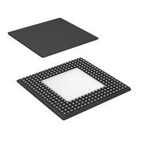
CYP15G0401RB-BGXC Cypress Semiconductor Corp, CYP15G0401RB-BGXC Datasheet - Page 7

CYP15G0401RB-BGXC
Manufacturer Part Number
CYP15G0401RB-BGXC
Description
IC RECEIVER HOTLINK 256LBGA
Manufacturer
Cypress Semiconductor Corp
Series
HOTlink II™r
Type
Transceiverr
Datasheet
1.CYP15G0401RB-BGXC.pdf
(35 pages)
Specifications of CYP15G0401RB-BGXC
Package / Case
256-LBGA Exposed Pad, 32-HLBGA
Number Of Drivers/receivers
0/4
Protocol
Multiprotocol
Voltage - Supply
3.135 V ~ 3.465 V
Mounting Type
Surface Mount
Product
PHY
Data Rate
1500 MBd
Supply Voltage (max)
3.465 V
Supply Voltage (min)
3.135 V
Supply Current
0.69 A
Maximum Operating Temperature
+ 70 C
Minimum Operating Temperature
0 C
Mounting Style
SMD/SMT
Number Of Channels
4RX
Lead Free Status / RoHS Status
Lead free / RoHS Compliant
Lead Free Status / RoHS Status
Lead free / RoHS Compliant, Lead free / RoHS Compliant
Available stocks
Company
Part Number
Manufacturer
Quantity
Price
Company:
Part Number:
CYP15G0401RB-BGXC
Manufacturer:
Cypress Semiconductor Corp
Quantity:
10 000
Document #: 38-02111 Rev. **
Pin Descriptions
CYP15G0401RB Quad HOTLink II Receiver
Receive Path Data Signals
RXDA[7:0]
RXDB[7:0]
RXDC[7:0]
RXDD[7:0]
RXSTA[2:
0]
RXSTB[2:
0]
RXSTC[2:
0]
RXSTD[2:
0]
RXOPA
RXOPB
RXOPC
RXOPD
Receive Path Clock and Clock Control
RXRATE
TRGRATE LVTTL Input,
FRAMCH
AR
RFEN
Notes:
Pin Name
2. When TRGCLK is configured for half-rate operation (TRGRATE = HIGH), these inputs are sampled (or the outputs change) relative to both the rising and falling
3. Three-level select inputs are used for static configuration. They are ternary (not binary) inputs that make use of non-standard logic levels of LOW, MID, and
edges of TRGCLK.
HIGH. The LOW level is usually implemented by direct connection to V
not connected or allowed to float, a Three-level select input will self-bias to the MID level.
LVTTL Output,
synchronous to the
selected RXCLKx↑ output
(or TRGCLK↑ input
when RXCKSEL = LOW)
LVTTL Output,
synchronous to the
selected RXCLKx↑ output
(or TRGCLK↑ input
when RXCKSEL = LOW)
Three-state, LVTTL
Output, synchronous to
the selected
RXCLKx↑ output
(or TRGCLK↑ input
when RXCKSEL = LOW)
LVTTL Input, static control
input, internal pull-down
static control input,
internal pull-down
Three-level Select
static control input
LVTTL Input,
asynchronous,
internal pull-down
I/O Characteristics
[3]
[2]
[2]
[2]
,
Parallel Data Output. These outputs change following the rising edge of the selected
receive interface clock.
When the Decoder is enabled (DECMODE = HIGH or MID), these outputs represent
either received data or special characters. The status of the received data is represented
by the values of RXSTx[2:0].
When the Decoder is bypassed (DECMODE = LOW), RXDx[7:0] become the higher order
bits of the 10-bit received character. See Table 7 for details.
Parallel Status Output. These outputs change following the rising edge of the selected
receive interface clock.
When the Decoder is bypassed (DECMODE = LOW), RXSTx[1:0] become the two
low-order bits of the 10-bit received character, while RXSTx[2] = HIGH indicates the
presence of a Comma character in the Output Register. See Table 7 for details.
When the Decoder is enabled (DECMODE = HIGH or MID), RXSTx[2:0] provide status
of the received signal. See Table 9 and Table 10 for a list of Receive Character status.
Receive Path Odd Parity. When parity generation is enabled (PARCTL ≠ LOW), the
parity output at these pins is valid for the data on the associated RXDx bus bits. When
parity generation is disabled (PARCTL = LOW) these output drivers are disabled (High-Z).
Receive Clock Rate Select. When LOW, the RXCLKx± recovered clock outputs are
complementary clocks operating at the recovered character rate. Data for the associated
receive channels should be latched on the rising edge of RXCLKx+ or falling edge of
RXCLKx–.
When HIGH, the RXCLKx± recovered clock outputs are complementary clocks operating
at half the character rate. Data for the associated receive channels should be latched
alternately on the rising edge of RXCLKx+ and RXCLKx–.
When TRGCLK± is selected to clock the output registers (RXCKSELx = LOW), RXRATEx
is not interpreted. The RXCLKA± and RXCLKC± output clocks will follow the frequency
and duty cycle of TRGCLK±.
Training Clock Rate Select. When TRGCLK is selected to clock the receive parallel
interfaces (RXCKSEL = LOW), the TRGRATE input also determines if the clocks on the
RXCLKA± and RXCLKC± outputs are full or half-rate. When TRGRATE = HIGH
(TRGCLK is half-rate) and RXCKSEL = LOW, the RXCLKA± and RXCLKC± output clocks
are also half-rate clocks and follow the frequency and duty cycle of the TRGCLK input.
When TRGRATE = LOW (TRGCLK is full-rate) and RXCKSEL = LOW, the RXCLKA± and
RXCLKC± output clocks are full-rate clocks and follow the frequency and duty cycle of
the TRGCLK input.
Framing Character Select. Used to select the character or portion of a character used
for character framing of the received data streams. When MID, the Framer looks for both
positive and negative disparity versions of the eight-bit Comma character. When HIGH,
the Framer looks for both positive and negative disparity versions of the K28.5 character.
Configuring FRAMCHAR to LOW is reserved for component test.
Reframe Enable for All Channels. Active HIGH. When HIGH, the framers in all four
channels are enabled to frame per the presently enabled framing mode as selected by
RFMODE and selected framing character as selected by FRAMCHAR.
PRELIMINARY
SS
(ground). The HIGH level is usually implemented by direct connection to V
Signal Description
CYP15G0401RB
Page 7 of 35
CC
. When
[+] Feedback


