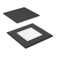
CYP15G0401RB-BGXC Cypress Semiconductor Corp, CYP15G0401RB-BGXC Datasheet - Page 20

CYP15G0401RB-BGXC
Manufacturer Part Number
CYP15G0401RB-BGXC
Description
IC RECEIVER HOTLINK 256LBGA
Manufacturer
Cypress Semiconductor Corp
Series
HOTlink II™r
Type
Transceiverr
Datasheet
1.CYP15G0401RB-BGXC.pdf
(35 pages)
Specifications of CYP15G0401RB-BGXC
Package / Case
256-LBGA Exposed Pad, 32-HLBGA
Number Of Drivers/receivers
0/4
Protocol
Multiprotocol
Voltage - Supply
3.135 V ~ 3.465 V
Mounting Type
Surface Mount
Product
PHY
Data Rate
1500 MBd
Supply Voltage (max)
3.465 V
Supply Voltage (min)
3.135 V
Supply Current
0.69 A
Maximum Operating Temperature
+ 70 C
Minimum Operating Temperature
0 C
Mounting Style
SMD/SMT
Number Of Channels
4RX
Lead Free Status / RoHS Status
Lead free / RoHS Compliant
Lead Free Status / RoHS Status
Lead free / RoHS Compliant, Lead free / RoHS Compliant
Available stocks
Company
Part Number
Manufacturer
Quantity
Price
Company:
Part Number:
CYP15G0401RB-BGXC
Manufacturer:
Cypress Semiconductor Corp
Quantity:
10 000
Document #: 38-02111 Rev. **
Maximum Ratings
(Above which the useful life may be impaired. User guidelines
only, not tested.)
Storage Temperature .................................. –65°C to +150°C
Ambient Temperature with Power Applied....–55°C to +125°C
Supply Voltage to Ground Potential ............... –0.5V to +3.8V
DC Voltage Applied to LVTTL Outputs
in High-Z State .......................................–0.5V to V
Output Current into LVTTL Outputs (LOW)..................60 mA
DC Input Voltage....................................–0.5V to V
CYP15G0401RB DC Electrical Characteristics
V
V
I
I
V
V
I
I
I
I
V
V
V
V
V
V
V
I
I
I
V
V
Notes:
12. Tested one output at a time, output shorted for less than one second, less than 10% duty cycle.
13. This is the minimum difference in voltage between the true and complement inputs required to ensure detection of a logic-1 or logic-0. A logic-1 exists when the
14. The common mode range defines the allowable range of TRGCLK+ and TRGCLK− when TRGCLK+ = TRGCLK−. This marks the zero-crossing between the
OST
OZL
IHT
ILT
IHPDT
ILPUT
IHH
IMM
ILL
LVTTL-compatible Outputs
LVTTL-compatible Inputs
LVDIFF Inputs: TRGCLK±
Three-level Inputs
Differential Serial Line Receiver Inputs: INA1±, INA2±, INB1±, INB2±, INC1±, INC2±, IND1±, IND2±
Parameter
OHT
OLT
IHT
ILT
DIFF
IHHP
ILLP
COMREF
IHH
IMM
ILL
DIFFS
IHE
true (+) input is more positive than the complement (−) input. A logic-0 exists when the complement (−) input is more positive than true (+) input.
true and complement inputs as the signal switches between a logic-1 and a logic-0.
[13]
[13]
[14]
Output HIGH Voltage
Output LOW Voltage
Output Short Circuit Current
High-Z Output Leakage Current
Input HIGH Voltage
Input LOW Voltage
Input HIGH Current
Input LOW Current
Input HIGH Current with internal pull-down V
Input LOW Current with internal pull-up
Input Differential Voltage
Highest Input HIGH Voltage
Lowest Input LOW voltage
Common Mode Range
Three-level Input HIGH Voltage
Three-level Input MID Voltage
Three-level Input LOW Voltage
Input HIGH Current
Input MID current
Input LOW current
Input Differential Voltage |(IN+) − (IN−)|
Highest Input HIGH Voltage
Description
CC
CC
PRELIMINARY
+ 0.5V
+ 0.5V
I
I
V
TRGCLK Input, V
Other Inputs, V
TRGCLK Input, V
Other Inputs, V
V
Min. ≤ V
Min. ≤ V
Min. ≤ V
V
V
V
OH
OL
OUT
IN
IN
IN
IN
IN
Over the Operating Range
= 4 mA, V
= −4 mA, V
= V
= 0.0V
= V
= V
= GND
= 0V
CC
CC
CC
Static Discharge Voltage........................................... > 2000V
(per MIL-STD-883, Method 3015)
Latch-up Current..................................................... > 200 mA
Power-up Requirements
The CYP15G0401RB requires one power-supply. The voltage
on any input or I/O pin cannot exceed the power pin during
power-up
Commercial
Industrial
CC
CC
CC
Operating Range
Test Conditions
/2
[12]
≤ Max.
≤ Max.
≤ Max.
Range
CC
CC
IN
IN
= Min.
= Min.
= V
= 0.0V
IN
IN
= V
= 0.0V
CC
CC
Ambient Temperature
–40°C to +85°C
0°C to +70°C
0.87 * V
0.47 * V
Min.
CYP15G0401RB
–0.5
–20
–20
400
–50
100
2.4
2.0
1.2
0.0
1.0
0.0
0
CC
CC
V
0.53 * V
0.13 * V
V
CC
CC
V
Max.
–100
+200
–200
–200
1200
–1.5
V
V
V
V
V
+40
–40
200
0.4
0.8
1.5
20
CC/2
50
Page 20 of 35
– 1.2V
CC
CC
CC
CC
CC
+3.3V ±5%
+3.3V ±5%
+ 0.3
CC
CC
V
CC
Unit
mA
mA
mA
mV
mV
µA
µA
µA
µA
µA
µA
µA
µA
V
V
V
V
V
V
V
V
V
V
V
[+] Feedback


