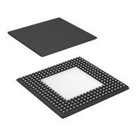
CYP15G0401RB-BGXC Cypress Semiconductor Corp, CYP15G0401RB-BGXC Datasheet - Page 16

CYP15G0401RB-BGXC
Manufacturer Part Number
CYP15G0401RB-BGXC
Description
IC RECEIVER HOTLINK 256LBGA
Manufacturer
Cypress Semiconductor Corp
Series
HOTlink II™r
Type
Transceiverr
Datasheet
1.CYP15G0401RB-BGXC.pdf
(35 pages)
Specifications of CYP15G0401RB-BGXC
Package / Case
256-LBGA Exposed Pad, 32-HLBGA
Number Of Drivers/receivers
0/4
Protocol
Multiprotocol
Voltage - Supply
3.135 V ~ 3.465 V
Mounting Type
Surface Mount
Product
PHY
Data Rate
1500 MBd
Supply Voltage (max)
3.465 V
Supply Voltage (min)
3.135 V
Supply Current
0.69 A
Maximum Operating Temperature
+ 70 C
Minimum Operating Temperature
0 C
Mounting Style
SMD/SMT
Number Of Channels
4RX
Lead Free Status / RoHS Status
Lead free / RoHS Compliant
Lead Free Status / RoHS Status
Lead free / RoHS Compliant, Lead free / RoHS Compliant
Available stocks
Company
Part Number
Manufacturer
Quantity
Price
Company:
Part Number:
CYP15G0401RB-BGXC
Manufacturer:
Cypress Semiconductor Corp
Quantity:
10 000
Document #: 38-02111 Rev. **
.
Table 7. Decoder Bypass Mode (DECMODE = LOW)
When the Cypress or Alternate Mode Framer is enabled and
half-rate
(RFMODE ≠ LOW and RXRATE = HIGH), the output clock is
not modified when framing is detected, but a single pipeline
stage may be added or subtracted from the data stream by the
Framer logic such that the rising edge of RXCLKx+ occurs
when COMDETx is present on the associated output bus.
This adjustment only occurs when the Framer is enabled
(RFEN = HIGH). When the Framer is disabled, the clock
boundaries are not adjusted, and COMDETx may be asserted
during the rising edge of RXCLK– (if an odd number of
characters were received following the initial framing).
Parity Generation
In addition to the eleven data and status bits that are presented
by each channel, an RXOPx parity output is also available on
each channel. This allows the CYP15G0401RB to support
ODD parity generation for each channel. To handle a wide
range of system environments, the CYP15G0401RB supports
different forms of parity generation, including no parity.
When the decoders are enabled (DECMODE ≠ LOW), parity
can be generated on
When the decoders are bypassed (DECMODE = LOW), parity
can be generated on
These modes differ in the number of bits which are included in
the parity calculation. Only ODD parity is provided which
ensures that at least one bit of the data bus is always a logic-1.
Those bits covered by parity generation are listed in Table 8.
Notes:
10. Receive path parity output drivers (RXOPx) are disabled (High-Z) when PARCTL = LOW.
11. When the Decoder is bypassed (DECMODE = LOW) and BIST is not enabled (Receive BIST Latch output is HIGH), RXSTx[2] is driven to a logic-0, except when
• the RXDx[7:0] character
• the RXDx[7:0] character and RXSTx[2:0] status.
• the RXDx[7:0] and RXSTx[1:0] bits
• the RXDx[7:0] and RXSTx[2:0] bits.
RXSTx[2]
the character in the output buffer is a framing character.
RXDx[7]
Signal Name
RXSTx[1]
RXSTx[0]
RXDx[0]
RXDx[1]
RXDx[2]
RXDx[3]
RXDx[4]
RXDx[5]
RXDx[6]
receive
(MSB)
(LSB)
port
Bus Weight
COMDETx
2
2
2
2
2
2
2
2
2
2
clocking
0
1
2
3
4
5
6
7
8
9
is
10Bit Name
also
a
b
c
d
e
g
h
i
f
j
PRELIMINARY
enabled
Table 8. Output Register Parity Generation
Parity generation is enabled through the three-level select
PARCTL input. When PARCTL = LOW, parity checking is
disabled, and the RXOPx outputs are all disabled (High-Z).
When PARCTL = MID (open) and the decoders are enabled
(DECMODE ≠ LOW), ODD parity is generated for the received
and decoded character in the RXDx[7:0] signals and is
presented
PARCTL = MID
(DECMODE = LOW), ODD parity is generated for the received
and decoded character in the RXDx[7:0] and RXSTx[1:0] bit
positions. When PARCTL = HIGH, ODD parity is generated for
the RXDx[7:0] and the associated RXSTx[2:0] status bits.
Receive Status Bits
When the 10B/8B Decoder is enabled (DECMODE ≠ LOW),
each character presented at the Output Register includes
three associated status bits. These bits are used to identify:
These conditions normally overlap; e.g., a valid data character
received with incorrect running disparity is not reported as a
valid data character. It is instead reported as a Decoder
violation of some specific type. This implies a hierarchy or
priority level to the various status bit combinations. The
hierarchy and value of each status is listed in Table 9.
The receive status when normal data is received is shown in
Table 9. The receive status when Receive BIST is enabled is
shown in Table 10.
• if the contents of the data bus are valid
• the type of character present
• the state of receive BIST operations (regardless of the state
• character violations.
RXSTx[2]
RXSTx[1]
RXSTx[0]
RXDx[0]
RXDx[1]
RXDx[2]
RXDx[3]
RXDx[4]
RXDx[5]
RXDx[6]
RXDx[7]
of DECMODE)
Signal
Name
on
Receive Parity Generate Mode (PARCTL)
LOW
[10]
the
and
associated
DECMODE
the
= LOW
X
X
X
X
X
X
X
X
X
X
decoders
CYP15G0401RB
MID
RXOPx
DECMODE
≠ LOW
X
X
X
X
X
X
X
X
are
output. When
Page 16 of 35
bypassed
HIGH
X
X
X
X
X
X
X
X
X
X
X
[11]
[+] Feedback


