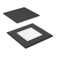
CYP15G0401RB-BGXC Cypress Semiconductor Corp, CYP15G0401RB-BGXC Datasheet - Page 18

CYP15G0401RB-BGXC
Manufacturer Part Number
CYP15G0401RB-BGXC
Description
IC RECEIVER HOTLINK 256LBGA
Manufacturer
Cypress Semiconductor Corp
Series
HOTlink II™r
Type
Transceiverr
Datasheet
1.CYP15G0401RB-BGXC.pdf
(35 pages)
Specifications of CYP15G0401RB-BGXC
Package / Case
256-LBGA Exposed Pad, 32-HLBGA
Number Of Drivers/receivers
0/4
Protocol
Multiprotocol
Voltage - Supply
3.135 V ~ 3.465 V
Mounting Type
Surface Mount
Product
PHY
Data Rate
1500 MBd
Supply Voltage (max)
3.465 V
Supply Voltage (min)
3.135 V
Supply Current
0.69 A
Maximum Operating Temperature
+ 70 C
Minimum Operating Temperature
0 C
Mounting Style
SMD/SMT
Number Of Channels
4RX
Lead Free Status / RoHS Status
Lead free / RoHS Compliant
Lead Free Status / RoHS Status
Lead free / RoHS Compliant, Lead free / RoHS Compliant
Available stocks
Company
Part Number
Manufacturer
Quantity
Price
Company:
Part Number:
CYP15G0401RB-BGXC
Manufacturer:
Cypress Semiconductor Corp
Quantity:
10 000
Document #: 38-02111 Rev. **
BIST Status State Machine
When a receive path is enabled to look for and compare the
received data stream with the BIST pattern, the RXSTx[2:0]
bits identify the present state of the BIST compare operation.
The BIST state machine has multiple states, as shown in
Figure 2 and Table 10. When the receive PLL detects an
out-of-lock condition, the BIST state is forced to the
Start-of-BIST state, regardless of the present state of the BIST
state machine. If the number of detected errors ever exceeds
the number of valid matches by greater than sixteen, the state
machine is forced to the WAIT_FOR_BIST state where it
monitors the interface for the first character (D0.0) of the next
BIST sequence. Also, if the Elasticity Buffer ever hits an
overflow/underflow condition, the status is forced to the
BIST_START until the buffer is recentered (approximately nine
character periods).
To ensure compatibility between the source and destination
systems when operating in BIST modes, the sending and
receiving ends of the link must use the same receive clock
setup, i.e. RXCKSEL = MID or RXCKSEL ≠ MID. This is appli-
PRELIMINARY
cable when interfacing to a CYP(V)15G0401DXB for example.
When interfacing to transmitter only HOTLink II devices such
as the CYP15G0401TB it is necessary to have RXCKSEL =
MID.
JTAG Support
The CYP15G0401RB contains a JTAG port to allow system
level diagnosis of device interconnect. Of the available JTAG
modes, only boundary scan is supported. This capability is
present only on the LVTTL inputs, LVTTL outputs and the
TRGCLK± clock input. The high-speed serial inputs and
outputs are not part of the JTAG test chain.
JTAG ID
The JTAG device ID for the CYP15G0401RB is ‘1C800069’x.
Three-level Select Inputs
Each Three-level select input reports as two bits in the scan
register. These bits report the LOW, MID, and HIGH state of
the associated input as 00, 10, and 11, respectively.
CYP15G0401RB
Page 18 of 35
[+] Feedback


