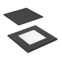
CYP15G0401RB-BGXC Cypress Semiconductor Corp, CYP15G0401RB-BGXC Datasheet - Page 9

CYP15G0401RB-BGXC
Manufacturer Part Number
CYP15G0401RB-BGXC
Description
IC RECEIVER HOTLINK 256LBGA
Manufacturer
Cypress Semiconductor Corp
Series
HOTlink II™r
Type
Transceiverr
Datasheet
1.CYP15G0401RB-BGXC.pdf
(35 pages)
Specifications of CYP15G0401RB-BGXC
Package / Case
256-LBGA Exposed Pad, 32-HLBGA
Number Of Drivers/receivers
0/4
Protocol
Multiprotocol
Voltage - Supply
3.135 V ~ 3.465 V
Mounting Type
Surface Mount
Product
PHY
Data Rate
1500 MBd
Supply Voltage (max)
3.465 V
Supply Voltage (min)
3.135 V
Supply Current
0.69 A
Maximum Operating Temperature
+ 70 C
Minimum Operating Temperature
0 C
Mounting Style
SMD/SMT
Number Of Channels
4RX
Lead Free Status / RoHS Status
Lead free / RoHS Compliant
Lead Free Status / RoHS Status
Lead free / RoHS Compliant, Lead free / RoHS Compliant
Available stocks
Company
Part Number
Manufacturer
Quantity
Price
Company:
Part Number:
CYP15G0401RB-BGXC
Manufacturer:
Cypress Semiconductor Corp
Quantity:
10 000
Document #: 38-02111 Rev. **
Pin Descriptions
CYP15G0401RB Quad HOTLink II Receiver
PARCTL
SPDSEL
TRSTZ
TRGCLK± Differential LVPECL or
INA1±
INB1±
INC1±
IND1±
INA2±
INB2±
INC2±
IND2±
INSELA
INSELB
INSELC
INSELD
SDASEL
BISTLE
Pin Name
Device Control Signals
Analog I/O and Control
Three-level Select
static control input
Three-level Select
static control input
LVTTL Input,
internal pull-up
single-ended
LVTTL Input Clock
LVPECL Differential Input Primary Differential Serial Data Inputs. These inputs accept the serial data stream for
LVPECL Differential Input Secondary Differential Serial Data Inputs. These inputs accept the serial data stream
LVTTL Input,
asynchronous
Three-level Select
static configuration input
LVTTL Input,
asynchronous,
internal pull-up
I/O Characteristics
(continued)
[3]
[3]
[3]
,
Parity Generate Control. Used to control the different parity generate functions. When
LOW, parity checking is disabled, and the RXOPx outputs are all disabled (High-Z). When
MID, and the 10B/8B Decoder is enabled (DECMODE ≠ LOW), ODD parity is generated
for the RXDx[7:0] outputs and presented on RXOPx. When the Decoder is disabled
(DECMODE = LOW), ODD parity is generated for the RXDx[7:0] and RXSTx[1:0] outputs
and presented on RXOPx. When HIGH, parity generation is enabled. ODD parity is
generated for the RXDx[7:0] and RXSTx[2:0] outputs and presented on RXOPx. See
Table 8 for details.
Serial Rate Select. This input specifies the operating bit-rate range of the receive PLLs.
LOW = 195–400 MBd, MID = 400–800 MBd, HIGH = 800–1500 MBd. When SPDSEL is
LOW, setting TRGRATE = HIGH (Half-rate Training Clock) is invalid.
Device Reset. Active LOW. Initializes all state machines and counters in the device.
When sampled LOW by the rising edge of TRGCLK↑, this input resets the internal state
machines and sets the Elasticity Buffer pointers to a nominal offset. When the reset is
removed (TRSTZ sampled HIGH by TRGCLK↑), the status and data outputs will become
deterministic in less than 16 TRGCLK cycles. The BISTLE and RXLE latches are reset
by TRSTZ. If the Elasticity Buffer is used, TRSTZ should be applied after power up to
initialize the internal pointers into these memory arrays.
Training Clock. This clock is used as the centering frequency of the Range Controller
block of the Receive CDR PLLs, via the Clock Multiplier. This input clock may also be
selected to clock the receive parallel interfaces. When driven by a single-ended LVCMOS
or LVTTL clock source, connect the clock source to either the true or complement
TRGCLK input, and leave the alternate TRGCLK input open (floating). When driven by
an LVPECL clock source, the clock must be a differential clock, using both inputs. When
RXCKSEL = LOW, the Elasticity Buffer is enabled and TRGCLK is used as the clock for
the parallel receive data (output) interface.
If the Elasticity Buffer is used, framing characters will be inserted or deleted to/from the
data stream to compensate for frequency differences between the training clock and
recovered clock. When an addition happens, a K28.5 will be appended immediately after
a framing character is detected in the Elasticity Buffer. When deletion happens, a framing
character will be removed from the data stream when detected in the Elasticity Buffer.
deserialization and decoding. The INx1± serial streams are passed to the receiver Clock
and Data Recovery (CDR) circuits to extract the data content when INSELx = HIGH.
for deserialization and decoding. The INx2± serial streams are passed to the receiver
Clock and Data Recovery (CDR) circuits to extract the data content when INSELx = LOW.
Receive Input Selector. Determines which external serial bit stream is passed to the
receiver Clock and Data Recovery circuit. When HIGH, the INx1± input is selected. When
LOW, the INx2± input is selected.
Signal Detect Amplitude Level Select. Allows selection of one of three predefined
amplitude trip points for a valid signal indication, as listed in Table 1.
Receive BIST Latch Enable. Active HIGH. When BISTLE = HIGH, the signals on the
BRE[3:0] inputs directly control the receive BIST enables. When the BRE[x] input is LOW,
the associated receive channel is configured to compare the BIST sequence. When the
BRE[x] input is HIGH, the associated receive channel is configured for normal data
reception. The specific mapping of BRE[3:0] signals to receive BIST enables is listed in
Table 2. When BISTLE returns LOW, the last values present on BRE[3:0] are captured
in the internal BIST Enable Latch. When the latch is closed, if the device is reset (TRSTZ
is sampled LOW), the latch is reset to disable BIST on all receive channels.
PRELIMINARY
Signal Description
CYP15G0401RB
Page 9 of 35
[+] Feedback


