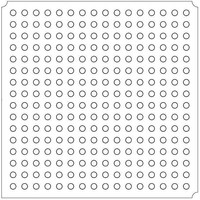
CYP15G0401DXB-BGC Cypress Semiconductor Corp, CYP15G0401DXB-BGC Datasheet - Page 15

CYP15G0401DXB-BGC
Manufacturer Part Number
CYP15G0401DXB-BGC
Description
IC TXRX HOTLINK 256LBGA
Manufacturer
Cypress Semiconductor Corp
Series
HOTlink II™r
Type
Transceiverr
Datasheet
1.CYW15G0401DXB-BGXC.pdf
(53 pages)
Specifications of CYP15G0401DXB-BGC
Package / Case
256-LBGA Exposed Pad, 32-HLBGA
Number Of Drivers/receivers
4/4
Protocol
Multiprotocol
Voltage - Supply
3.135 V ~ 3.465 V
Mounting Type
Surface Mount
Product
PHY
Supply Voltage (min)
3.135 V
Supply Current
1.06 A
Maximum Operating Temperature
+ 70 C
Minimum Operating Temperature
0 C
Mounting Style
SMD/SMT
Number Of Channels
4
Lead Free Status / RoHS Status
Lead free / RoHS Compliant
For Use With
CYP15G0401DX-EVAL - IC TXRX HOTLINK 256-BGA
Lead Free Status / RoHS Status
Lead free / RoHS Compliant, Lead free / RoHS Compliant
Available stocks
Company
Part Number
Manufacturer
Quantity
Price
Company:
Part Number:
CYP15G0401DXB-BGC
Manufacturer:
CY
Quantity:
767
Company:
Part Number:
CYP15G0401DXB-BGC
Manufacturer:
CYPRESS
Quantity:
586
Company:
Part Number:
CYP15G0401DXB-BGC
Manufacturer:
Cypress Semiconductor Corp
Quantity:
10 000
Part Number:
CYP15G0401DXB-BGC
Manufacturer:
CYPRESS/赛普拉斯
Quantity:
20 000
Document #: 38-02002 Rev. *L
Pin Descriptions
CYP(V)(W)15G0401DXB Quad HOTLink II Transceiver
CYP(V)(W)15G0401DXB
The CYP(V)(W)15G0401DXB is a highly configurable device
designed to support reliable transfer of large quantities of data,
using high-speed serial links, from one or multiple sources to
one or multiple destinations. This device supports four
single-byte or single-character channels that may be
combined to support transfer of wider buses.
CYP(V)(W)15G0401DXB Transmit Data Path
Operating Modes
The transmit path of the CYP(V)(W)15G0401DXB supports
four character-wide data paths. These data paths are used in
multiple operating modes as controlled by the TXMODE[1:0]
inputs.
Input Register
The bits in the Input Register for each channel support
different assignments, based on if the character is unencoded,
encoded with two control bits, or encoded with three control
bits. These assignments are shown in Table 1. Each Input
MASTER
BOND_ALL
BOND_INH
JTAG Interface
TMS
TCLK
TDO
TDI
Power
V
GND
CC
Pin Name
LVTTL Input,
static configuration input,
internal pull-down
Bidirectional Open Drain,
Internal pull-up
LVTTL Input,
static configuration input,
Internal pull-up
LVTTL Input,
internal pull-up
LVTTL Input,
internal pull-down
Three-state
LVTTL Output
LVTTL Input, internal pull-up Test Data In. JTAG data input port.
I/O Characteristics
(continued)
HOTLink II Operation
Master Device Select. When LOW, the present device is configured as the master,
and BONDST[1:0] outputs are driven. When HIGH, the present device is configured
as a slave, and BONDST[1:0] are inputs. MASTER is only interpreted when
configured for quad channel bonding, and the receive parallel interface is clocked by
REFCLK↑.
All Channels Bonded Indicator. Active HIGH, wired AND. BOND_ALL pins from all
CYP(V)15G0401DXB devices in the same bonding domain must be wired together. After
bonding resolution is completed and when HIGH, all receive channels have detected valid
framing. This output is LOW during the bonding resolution process. This output is driven
only when configured for four channel bonding, and the receive parallel interface is
clocked by REFCLK↑.
Parallel Bond Inhibit. Active LOW. When asserted (LOW), this signal inhibits the
adjustment of character offsets in all receive channels if the Bonding Sequence has
not been detected in all bonded channels. When HIGH, all channels that have
detected the Bonding Sequence are allowed to align their Receive Elasticity Buffer
pipelines. For any channels to bond, the selected master channel must be a member
of the group. When multiple devices are used together, the BOND_INH input on all
parts must be configured the same.
Test Mode Select. Used to control access to the JTAG Test Modes. If maintained high
for ≥5 TCLK cycles, the JTAG test controller is reset. The TAP controller is also reset
automatically upon application of power to the device.
JTAG Test Clock
Test Data Out. JTAG data output buffer which is High-Z while JTAG test mode is not
selected.
+3.3V Power
Signal and power ground for all internal circuits.
Register captures a minimum of eight data bits and two control
bits on each input clock cycle. When the Encoder is bypassed,
the TXCTx[1:0] control bits, are part of the preencoded 10-bit
character.
When the Encoder is enabled (TXMODE[1] ≠ LOW), the
TXCTx[1:0] bits are interpreted along with the associated
TXDx[7:0] character to generate the specific 10-bit trans-
mission character. When TXMODE[0] ≠ HIGH, an additional
special character select (SCSEL) input is also captured and
interpreted. This SCSEL input is used to modify the encoding
of the associated characters. When the transmit Input
Registers are clocked by a common clock (TXCLKA↑ or
REFCLK↑), this SCSEL input can be changed on a
clock-by-clock basis and affects all four channels.
When operated with a separate input clock on each transmit
channel, this SCSEL input is sampled synchronous to
TXCLKA↑. While the value on SCSEL still affects all channels,
it is interpreted when the character containing it is read from
the transmit Phase-align Buffer (where all four paths are inter-
nally clocked synchronously).
Signal Description
CYW15G0401DXB
CYP15G0401DXB
CYV15G0401DXB
Page 15 of 53


