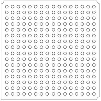
CYP15G0401DXB-BGC Cypress Semiconductor Corp, CYP15G0401DXB-BGC Datasheet - Page 37

CYP15G0401DXB-BGC
Manufacturer Part Number
CYP15G0401DXB-BGC
Description
IC TXRX HOTLINK 256LBGA
Manufacturer
Cypress Semiconductor Corp
Series
HOTlink II™r
Type
Transceiverr
Datasheet
1.CYW15G0401DXB-BGXC.pdf
(53 pages)
Specifications of CYP15G0401DXB-BGC
Package / Case
256-LBGA Exposed Pad, 32-HLBGA
Number Of Drivers/receivers
4/4
Protocol
Multiprotocol
Voltage - Supply
3.135 V ~ 3.465 V
Mounting Type
Surface Mount
Product
PHY
Supply Voltage (min)
3.135 V
Supply Current
1.06 A
Maximum Operating Temperature
+ 70 C
Minimum Operating Temperature
0 C
Mounting Style
SMD/SMT
Number Of Channels
4
Lead Free Status / RoHS Status
Lead free / RoHS Compliant
For Use With
CYP15G0401DX-EVAL - IC TXRX HOTLINK 256-BGA
Lead Free Status / RoHS Status
Lead free / RoHS Compliant, Lead free / RoHS Compliant
Available stocks
Company
Part Number
Manufacturer
Quantity
Price
Company:
Part Number:
CYP15G0401DXB-BGC
Manufacturer:
CY
Quantity:
767
Company:
Part Number:
CYP15G0401DXB-BGC
Manufacturer:
CYPRESS
Quantity:
586
Company:
Part Number:
CYP15G0401DXB-BGC
Manufacturer:
Cypress Semiconductor Corp
Quantity:
10 000
Part Number:
CYP15G0401DXB-BGC
Manufacturer:
CYPRESS/赛普拉斯
Quantity:
20 000
Document #: 38-02002 Rev. *L
CYP(V)(W)15G0401DXB
t
t
t
t
f
t
t
t
CYP(V)(W)15G0401DXB Receiver LVTTL Switching Characteristics Over the Operating Range
f
t
t
t
t
t
t
t
t
CYP(V)(W)15G0401DXB REFCLK Switching Characteristics Over the Operating Range
f
t
t
t
t
t
t
t
t
t
t
Notes:
33. The ratio of rise time to falling time must not vary by greater than 2:1.
34. For a given operating frequency, neither rise or fall specification can be greater than 20% of the clock-cycle period or the data sheet maximum time.
35. Parallel data output specifications are only valid if all inputs or outputs are loaded with similar DC and AC loads.
36. The duty cycle specification is a simultaneous condition with the t
37. Since this timing parameter is greater than the minimum time period of REFCLK it sets an upper limit to the frequency in which REFCLKx can be used to clock
TXCLKR
TXCLKF
TXDS
TXDH
TOS
TXCLKO
TXCLKOD+
TXCLKOD–
RS
RXCLKP
RXCLKH
RXCLKL
RXCLKD
RXCLKR
RXCLKF
RXDV–
RXDV+
REF
REFCLK
REFH
REFL
REFD
REFR
REFF
TREFDS
TREFDH
RREFDA
RREFDV
Parameter
cannot be as large as 30% – 70%.
the receive data out of the output register. For predictable timing, users can use this parameter only if REFCLK period is greater than sum of t
set-up time of the upstream device. When this condition is not true, RXCLKC± or RXCLKA± (a buffered or delayed version of REFCLK when RXCKSELx =
LOW) could be used to clock the receive data out of the device.
[32, 33, 34]
[36]
[32, 33, 34]
[32, 33, 34]
[35]
[35]
[32, 33, 34]
[32]
[37]
[32]
TXCLKx Rise Time
TXCLKx Fall Time
Transmit Data Set-Up Time to TXCLKx↑ (TXCKSEL ≠ LOW)
Transmit Data Hold Time from TXCLKx↑ (TXCKSEL ≠ LOW)
TXCLKO Clock Frequency = 1x or 2x REFCLK Frequency
TXCLKO Period
TXCLKO+ Duty Cycle with 60% HIGH time
TXCLKO– Duty Cycle with 40% HIGH time
RXCLKx Clock Output Frequency
RXCLKx Period
RXCLKx HIGH Time (RXRATE = LOW)
RXCLKx HIGH Time (RXRATE = HIGH)
RXCLKx LOW Time (RXRATE = LOW)
RXCLKx LOW Time (RXRATE = HIGH)
RXCLKx Duty Cycle centered at 50%
RXCLKx Rise Time
RXCLKx Fall Time
Status and Data Valid Time to RXCLKx (RXCKSEL HIGH or MID)
Status and Data Valid Time to RXCLKx (HALF RATE RECOVERED
CLOCK)
Status and Data Valid Time From RXCLKx (RXCKSEL HIGH or MID)
Status and Data Valid Time From RXCLKx (HALF RATE RECOVERED
CLOCK)
REFCLK Clock Frequency
REFCLK Period
REFCLK HIGH Time (TXRATE = HIGH)
REFCLK HIGH Time (TXRATE = LOW)
REFCLK LOW Time (TXRATE = HIGH)
REFCLK LOW Time (TXRATE = LOW)
REFCLK Duty Cycle
REFCLK Rise Time (20% – 80%)
REFCLK Fall Time (20% – 80%)
Transmit Data Setup Time to REFCLK (TXCKSEL = LOW)
Transmit Data Hold Time from REFCLK (TXCKSEL = LOW)
Receive Data Access Time from REFCLK (RXCKSEL = LOW)
Receive Data Valid Time from REFCLK (RXCKSEL = LOW)
AC Characteristics
Description
Over the Operating Range (continued)
REFH
and t
REFL
parameters. This means that at faster character rates the REFCLK duty cycle
5UI – 1.5
5UI – 1.0
5UI – 1.8
5UI – 2.3
2.33
2.33
6.66
6.66
6.66
CYW15G0401DXB
2.9
2.9
CYP15G0401DXB
CYV15G0401DXB
Min.
–1.0
–0.5
9.75
5.66
5.66
–1.0
19.5
0.2
0.2
1.7
0.8
0.3
0.3
5.9
5.9
1.7
0.8
2.5
20
30
[32]
[32]
[31]
[31]
[31]
[32]
[32]
102.56
150
150
150
26.64
52.28
26.64
52.28
51.28
Max.
+0.5
+1.0
+1.0
1.7
1.7
1.2
1.2
9.5
50
70
Page 37 of 53
2
2
[30]
[30]
[30]
RREFDA
MHz
MHz
MHz
and
Unit
ns
ns
ns
ns
ns
ns
ns
ns
ns
ns
ns
ns
ns
ns
ns
ns
ns
ns
ns
ns
ns
ns
ns
ns
ns
ns
ns
ns
ns
ns
%


