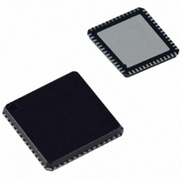
AD9991KCP Analog Devices Inc, AD9991KCP Datasheet - Page 22

AD9991KCP
Manufacturer Part Number
AD9991KCP
Description
IC CCD SIGNAL PROCESSOR 56-LFCSP
Manufacturer
Analog Devices Inc
Type
CCD Signal Processor, 10-Bitr
Datasheet
1.AD9991KCPZRL.pdf
(60 pages)
Specifications of AD9991KCP
Rohs Status
RoHS non-compliant
Input Type
Logic
Output Type
Logic
Interface
3-Wire Serial
Mounting Type
Surface Mount
Package / Case
56-LFCSP
Analog Front End Type
CCD
Analog Front End Category
Video
Interface Type
Serial (3-Wire)
Input Voltage Range
0.5V
Operating Supply Voltage (min)
2.7V
Operating Supply Voltage (typ)
3V
Operating Supply Voltage (max)
3.6V
Resolution
10b
Number Of Adc's
1
Power Supply Type
Analog/Digital
Operating Temp Range
-20C to 85C
Operating Temperature Classification
Commercial
Mounting
Surface Mount
Pin Count
56
Package Type
LFCSP EP
Number Of Channels
1
Current - Supply
-
Lead Free Status / RoHS Status
Not Compliant
Available stocks
Company
Part Number
Manufacturer
Quantity
Price
Company:
Part Number:
AD9991KCP
Manufacturer:
ADI
Quantity:
246
Company:
Part Number:
AD9991KCPZ
Manufacturer:
ADI
Quantity:
244
Company:
Part Number:
AD9991KCPZ-RL
Manufacturer:
FUJISU
Quantity:
4 000
The example shown in Figure 22 illustrates this operation. The
fi rst toggle position is 2, and the second toggle position is 9. In
non-Multiplier mode, this would cause the V-sequence to toggle
at pixel 2 and then pixel 9 within a single HD line. However,
toggle positions are now multiplied by the VTPLEN = 4, so the
fi rst toggle occurs at pixel count 8, and the second toggle occurs
at pixel count 36. Sweep mode has also been enabled to allow the
toggle positions to cross the HD line boundaries.
Vertical Sensor Gate (Shift Gate) Patterns
In an Interline CCD, the vertical sensor gates (VSG) are used
to transfer the pixel charges from the light-sensitive image area
into light-shielded vertical registers. From the light-shield verti-
cal registers, the image is then read out line-by-line by using the
vertical transfer pulses V1–V6 in conjunction with the high speed
horizontal clocks.
Register
SGPOL
SGTOG1
SGTOG2
AD9991
VSG PATTERNS
VPATLEN
NUMBER
V1–V6
PIXEL
HD
VD
HD
MULTIPLIER MODE V-PATTERN GROUP PROPERTIES:
1. START POLARITY (ABOVE: STARTPOL = 0)
2. FIRST, SECOND, AND THIRD TOGGLE POSITIONS (ABOVE: VTOG1 = 2, VTOG2 = 9)
3. LENGTH OF VPAT COUNTER (ABOVE: VPATLEN = 4). THIS IS THE MINIMUM RESOLUTION FOR TOGGLE POSITION CHANGES.
4. TOGGLE POSITIONS OCCUR AT LOCATION EQUAL TO (VTOG
5. IF SWEEP REGION IS ENABLED, THE V-PULSES MAY ALSO CROSS THE HD BOUNDRIES, AS SHOWN ABOVE
1
PROGRAMMABLE SETTINGS FOR EACH PATTERN:
1. START POLARITY OF PULSE
2. FIRST TOGGLE POSITION
3. SECOND TOGGLE POSITION
4. ACTIVE LINE FOR VSG PULSES WITHIN THE FIELD (PROGRAMMABLE IN THE FIELD REGISTER, NOT FOR EACH PATTERN)
1
1
2
2
Length
1b
12b
12b
3
3
3
START POSITION OF VPAT GROUP IS STILL PROGRAMMED IN THE V-SEQUENCE REGISTERS
Figure 22. Example of Multiplier Region for Wide Vertical Pulse Timing
4 1
4 5
Table IX. VSG Pattern Registers (also see Field Registers in Table VII)
2
6
3
7
4
8
4
Figure 23. Vertical Sensor Gate Pulse Placement
2
9 10 11 12 13 14 15 16 17 18 19 20 21 22 23 24 25 26 27 28 29 30 31 32 33 34 35 36 37 38 39 40
1
2
3
Range
High/Low
0–4095 Pixel Location
0–4095 Pixel Location
4
1
2
3
4
5
1
–22–
2
3
VPATLEN)
Table IX contains the summary of the VSG pattern registers. The
AD9991 has fi ve VSG outputs, VSG1–VSG5. Each of the out-
puts can be assigned to one of four programmed patterns by using
the SGPATSEL registers. Each pattern is generated in a similar
manner as the V-pattern groups, with a programmable start polar-
ity (SGPOL), fi rst toggle position (SGTOG1), and second toggle
position (SGTOG2). The active line where the VSG1–VSG5
pulses occur is programmable using the SGLINE1 and SGLINE2
registers. Additionally, any of the VSG1–VSG5 pulses may be
individually disabled by using the SGMASK register. The individ-
ual masking allows all of the SG patterns to be preprogrammed,
and the appropriate pulses for the different fi elds can be separately
enabled. For maximum fl exibility, the SGPATSEL, SGMASK,
and SGLINE registers are separately programmable for each fi eld.
More detail is given in the Complete Field section.
4
1
4
1
2
3
2
4
1
Description
Sensor Gate Starting Polarity for SG Pattern 0–3
First Toggle Position for SG Pattern 0–3
Second Toggle Position for SG Pattern 0–3
3
2
3
4 1
2
3
4 1
5
2
3
4 1
2
4
2
3
4
REV. 0


