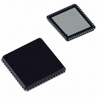
AD9991KCP Analog Devices Inc, AD9991KCP Datasheet - Page 41

AD9991KCP
Manufacturer Part Number
AD9991KCP
Description
IC CCD SIGNAL PROCESSOR 56-LFCSP
Manufacturer
Analog Devices Inc
Type
CCD Signal Processor, 10-Bitr
Datasheet
1.AD9991KCPZRL.pdf
(60 pages)
Specifications of AD9991KCP
Rohs Status
RoHS non-compliant
Input Type
Logic
Output Type
Logic
Interface
3-Wire Serial
Mounting Type
Surface Mount
Package / Case
56-LFCSP
Analog Front End Type
CCD
Analog Front End Category
Video
Interface Type
Serial (3-Wire)
Input Voltage Range
0.5V
Operating Supply Voltage (min)
2.7V
Operating Supply Voltage (typ)
3V
Operating Supply Voltage (max)
3.6V
Resolution
10b
Number Of Adc's
1
Power Supply Type
Analog/Digital
Operating Temp Range
-20C to 85C
Operating Temperature Classification
Commercial
Mounting
Surface Mount
Pin Count
56
Package Type
LFCSP EP
Number Of Channels
1
Current - Supply
-
Lead Free Status / RoHS Status
Not Compliant
Available stocks
Company
Part Number
Manufacturer
Quantity
Price
Company:
Part Number:
AD9991KCP
Manufacturer:
ADI
Quantity:
246
Company:
Part Number:
AD9991KCPZ
Manufacturer:
ADI
Quantity:
244
Company:
Part Number:
AD9991KCPZ-RL
Manufacturer:
FUJISU
Quantity:
4 000
Address Content Value
30
31
32
33
34
35
36
37
Address Content Value
40
41
42
Address Content Value
50
51
52
53
54
Address Content Value
60
61
62
63
64
65
66
REV. 0
Data Bit Default
[0]
[12:0]
[12:0]
[12:0]
[1:0]
[14:0]
[11:0]
[8:0]
Data Bit Default
[23:0]
[23:0]
[11:0]
Data Bit Default
[3:0]
[23:0]
[23:0]
[23:0]
[23:0]
Data Bit Default
[4:0]
[2:0]
[11:0]
[12]
[11:0]
[23:12]
[0]
[23:0]
[23:0]
0
01001
01001
00801
0
1249
00024
100
FFFFFF CLPMASK01
FFFFFF CLPMASK23
FFFFFF CLPMASK4
F
FFFFFF SGTOG12_0
FFFFFF SGTOG12_1
FFFFFF SGTOG12_2
FFFFFF SGTOG12_3
0
2
0
0
0
0
1
FFFFFF SUBCK1TOG
FFFFFF SUBCK2TOG
Register Name
CLIDIVIDE
H1CONTROL
H3CONTROL
RGCONTROL
HBLKRETIME
DRVCONTROL
SAMPCONTROL
DOUTCONTROL
Register Name
Register Name
SGPOL
Register Name
TRIGGER
READOUT
EXPOSURE
VDHDOFF
SUBCKSUPPRESS
SUBCKNUM
SUBCKPOL
Table XXII. Shutter Control Register Map
Table XX. CLPOB Masking Register Map
Table XIX. Timing Core Register Map
Table XXI. SG Pattern Register Map
Register Description
Divide CLI Input Clock by 2. 1 = Divide by 2.
H1 Signal Control: Polarity [0](0 = Inversion, 1 = No Inversion).
H1 Positive Edge Location [6:1]. H1 Negative Edge Location [12:7].
H3 Signal Control: Polarity [0](0 = Inversion, 1 = No Inversion).
H3 Positive Edge Location [6:1]. H3 Negative Edge Location [12:7].
RG Signal Control: Polarity [0](0 = Inversion, 1 = No Inversion).
RG Positive Edge Location [6:1]. RG Negative Edge Location [12:7].
Retime HBLK to Internal H1/H3 Clocks. H1 Retime [0]. H3 Retime [1].
Preferred setting is 1 for each bit. Setting each bit to 1 will add one cycle delay
to HBLK toggle positions.
Drive Strength Control for H1 [2:0], H2 [5:3], H3 [8:6], H4 [11:9], and
RG [14:12]. Drive Current Values: 0 = Off, 1 = 4.3 mA, 2 = 8.6 mA,
3 = 12.9 mA, 4 = 17.2 mA, 5 = 21.5 mA, 6 = 25.8 mA, 7 = 30.1 mA.
SHP/SHD Sample Control: SHP Sampling Location [5:0].
SHD Sampling Location [11:6].
DOUT Phase Control [5:0]. DCLK Mode [6]. DOUTDELAY [8:7].
Register Description
CLPOB Line Masking. Line #0 [11:0]. Line #1 [23:0].
CLPOB Line Masking. Line #2 [11:0]. Line #3 [23:0].
CLPOB Line Masking. Line #4 [11:0].
Register Description
Start Polarity for SG Patterns. Pattern #0 [0]. Pattern #1 [1].
Pattern #2 [2]. Pattern #3 [3].
Pattern #0. Toggle Position 1 [11:0]. Toggle Position 2 [23:12].
Pattern #1. Toggle Position 1 [11:0]. Toggle Position 2 [23:12].
Pattern #2. Toggle Position 1 [11:0]. Toggle Position 2 [23:12].
Pattern #3. Toggle Position 1 [11:0]. Toggle Position 2 [23:12].
Register Description
Trigger for VSUB [0], MSHUT [1], STROBE [2], Exposure [3], and
Readout [4]. Note that to trigger the Readout to automatically occur after the
Exposure period, both Exposure and Readout should be triggered together.
Number of Fields to Suppress the SUBCK Pulses after the VSG Line.
Number of Fields to Suppress the SUBCK and VSG Pulses.
Set = 1 to Disable the VD/HD Outputs during exposure (when >1 fi eld).
Number of SUBCK Pulses to Suppress after VSG Line.
Number of SUBCK Pulses per Field.
SUBCK Pulse Start Polarity.
First SUBCK Pulse. Toggle Position 1 [11:0]. Toggle Position 2 [23:0].
Second SUBCK Pulse. Toggle Position 1 [11:0]. Toggle Position 2 [23:0].
–41–
AD9991


