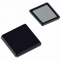
AD9991KCP Analog Devices Inc, AD9991KCP Datasheet - Page 32

AD9991KCP
Manufacturer Part Number
AD9991KCP
Description
IC CCD SIGNAL PROCESSOR 56-LFCSP
Manufacturer
Analog Devices Inc
Type
CCD Signal Processor, 10-Bitr
Datasheet
1.AD9991KCPZRL.pdf
(60 pages)
Specifications of AD9991KCP
Rohs Status
RoHS non-compliant
Input Type
Logic
Output Type
Logic
Interface
3-Wire Serial
Mounting Type
Surface Mount
Package / Case
56-LFCSP
Analog Front End Type
CCD
Analog Front End Category
Video
Interface Type
Serial (3-Wire)
Input Voltage Range
0.5V
Operating Supply Voltage (min)
2.7V
Operating Supply Voltage (typ)
3V
Operating Supply Voltage (max)
3.6V
Resolution
10b
Number Of Adc's
1
Power Supply Type
Analog/Digital
Operating Temp Range
-20C to 85C
Operating Temperature Classification
Commercial
Mounting
Surface Mount
Pin Count
56
Package Type
LFCSP EP
Number Of Channels
1
Current - Supply
-
Lead Free Status / RoHS Status
Not Compliant
Available stocks
Company
Part Number
Manufacturer
Quantity
Price
Company:
Part Number:
AD9991KCP
Manufacturer:
ADI
Quantity:
246
Company:
Part Number:
AD9991KCPZ
Manufacturer:
ADI
Quantity:
244
Company:
Part Number:
AD9991KCPZ-RL
Manufacturer:
FUJISU
Quantity:
4 000
Optical Black Clamp
The optical black clamp loop is used to remove residual offsets
in the signal chain and to track low frequency variations in the
CCD’s black level. During the optical black (shielded) pixel inter-
val on each line, the ADC output is compared with a fi xed black
level reference, selected by the user in the Clamp Level register.
The value can be programmed between 0 LSB and 63.75 LSB in
256 steps. The resulting error signal is fi ltered to reduce noise,
and the correction value is applied to the ADC input through a
D/A converter. Normally, the optical black clamp loop is turned
on once per horizontal line, but this loop can be updated more
slowly to suit a particular application. If external digital clamp-
ing is used during the postprocessing, the AD9991 optical black
clamping may be disabled using Bit D2 in the OPRMODE regis-
ter. When the loop is disabled, the Clamp Level register may still
be used to provide programmable offset adjustment.
The CLPOB pulse should be placed during the CCD’s optical
black pixels. It is recommended that the CLPOB pulse duration
AD9991
–32–
be at least 20 pixels wide to minimize clamp noise. Shorter pulse-
widths may be used, but clamp noise may increase, and the ability
to track low frequency variations in the black level will be reduced.
See the Horizontal Clamping and Blanking section and the Hori-
zontal Timing Sequence Example section for timing examples.
Digital Data Outputs
The AD9991 digital output data is latched using the DOUT
PHASE register value, as shown in Figure 33. Output data timing
is shown in Figure 8. It is also possible to leave the output latches
transparent so that the data outputs are valid immediately from
the A/D converter. Programming the AFE CONTROL register bit
D4 to a 1 will set the output latches transparent. The data outputs
can also be disabled (three-stated) by setting the AFE CONTROL
register bit D3 to a 1.
The data output coding is normally straight binary, but the coding
my be changed to gray coding by setting the AFE CONTROL
register Bit D5 to 1.
REV. 0


