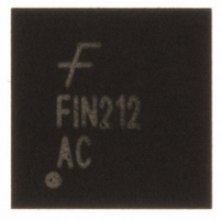
FIN212ACMLX Fairchild Semiconductor, FIN212ACMLX Datasheet - Page 12

FIN212ACMLX
Manufacturer Part Number
FIN212ACMLX
Description
IC SERIAL/DESERIAL 12BIT 32MLP
Manufacturer
Fairchild Semiconductor
Series
SerDes™r
Type
Serializer Deserializer with Multiple Frequency Ranger
Datasheet
1.FIN212ACGFX.pdf
(16 pages)
Specifications of FIN212ACMLX
Function
Serializer/Deserializer
Data Rate
560Mbps
Input Type
LVCMOS
Output Type
LVCMOS
Number Of Inputs
12
Number Of Outputs
12
Voltage - Supply
1.65 V ~ 3.6 V
Operating Temperature
-30°C ~ 70°C
Mounting Type
Surface Mount
Package / Case
32-MLP
No. Of Inputs
12
No. Of Outputs
12
Supply Voltage Range
2.5V To 3.6V, 1.65V To 3.6V
Driver Case Style
MLP
No. Of Pins
32
Termination Type
Solder
Operating Temperature Range
-30°C To +70°C
Rohs Compliant
Yes
Operating Supply Voltage
3.3 V
Maximum Power Dissipation
2.5 V to 3.6 V
Maximum Operating Temperature
+ 70 C
Minimum Operating Temperature
- 30 C
Mounting Style
SMD/SMT
Filter Terminals
Solder
Digital Ic Case Style
MLP
Lead Free Status / RoHS Status
Lead free / RoHS Compliant
Other names
FIN212ACMLXTR
Available stocks
Company
Part Number
Manufacturer
Quantity
Price
Company:
Part Number:
FIN212ACMLX
Manufacturer:
Freescale
Quantity:
162
Part Number:
FIN212ACMLX
Manufacturer:
FAIRCHILD/仙童
Quantity:
20 000
Tape and Reel Specifications
MLP Embossed Tape Dimensions
Notes:
A
requirements (see sketches A, B, and C).
MLP Shipping Reel Dimensions
© 2008 Fairchild Semiconductor Corporation
FIN212AC • Rev. 1.1.0
Tape Width
Package
0
, B
5 x 5
6 x 6
12
16
8
0
, and K
±0.1
5.35
5.35
A
Tc
T
0
0
K
Sketch A (Side or Front Sectional View)
0
330.0
330.0
330.0
Dia A
dimensions are determined with respect to the EIA/JEDEC RS-481 rotational and lateral movement
10° maximum component rotation
Max.
Dia A
max
Component Rotation
W
±0.1
5.35
5.35
B
c
0
Dim B
B
Min.
1.5
1.5
1.5
±0.5
1.55
1.55
0
D
Min.
1.50
1.50
D
1
+0.5/-0.2
Dia C
13.0
13.0
13.0
Figure 8. MLP Tape and Reel
A
W2 max Measured at Hub
B
0
±0.1
0
1.75
1.75
E
Component Rotation
Sketch B (Top View)
A
±0.1
5.50
5.50
P
0
See detail AA
F
0
10° maximum
Dia D
20.2
20.2
20.2
Min.
12
P
Typical component
cavity center line
Typical component
center line
Dia N
1
±0.1
1.40
1.40
K
0
D
D
1
Typ.
8.00
8.00
P
1
Dim N
178.0.
178.0.
178.0.
W3
Min.
W1 Measured at Hub
Dia D
Typ.
4.00
4.00
min
P
1.0mm
maximum
0
Component Lateral Movement
User Direction of Feed
Sketch C (Top View)
B Min
±0.5
Dim W1
2.00
2.00
+2.0/-0
P
12.4
16.4
2
8.4
DETAIL AA
P
2
1.0mm
maximum
Typ.
0.30
0.30
F
T
E
Dia C
Dim W2
14.4
18.4
22.4
±0/05
0.07
0.07
T
W
C
www.fairchildsemi.com
12.00
12.00
±0.3
W
11.9 ~ 15.4
15.9 ~ 19.4
(LSL-USL)
7.9 ~ 10.4
Dim W3
Typ.
9.30
9.30
W
C


