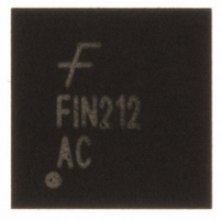
FIN212ACMLX Fairchild Semiconductor, FIN212ACMLX Datasheet - Page 5

FIN212ACMLX
Manufacturer Part Number
FIN212ACMLX
Description
IC SERIAL/DESERIAL 12BIT 32MLP
Manufacturer
Fairchild Semiconductor
Series
SerDes™r
Type
Serializer Deserializer with Multiple Frequency Ranger
Datasheet
1.FIN212ACGFX.pdf
(16 pages)
Specifications of FIN212ACMLX
Function
Serializer/Deserializer
Data Rate
560Mbps
Input Type
LVCMOS
Output Type
LVCMOS
Number Of Inputs
12
Number Of Outputs
12
Voltage - Supply
1.65 V ~ 3.6 V
Operating Temperature
-30°C ~ 70°C
Mounting Type
Surface Mount
Package / Case
32-MLP
No. Of Inputs
12
No. Of Outputs
12
Supply Voltage Range
2.5V To 3.6V, 1.65V To 3.6V
Driver Case Style
MLP
No. Of Pins
32
Termination Type
Solder
Operating Temperature Range
-30°C To +70°C
Rohs Compliant
Yes
Operating Supply Voltage
3.3 V
Maximum Power Dissipation
2.5 V to 3.6 V
Maximum Operating Temperature
+ 70 C
Minimum Operating Temperature
- 30 C
Mounting Style
SMD/SMT
Filter Terminals
Solder
Digital Ic Case Style
MLP
Lead Free Status / RoHS Status
Lead free / RoHS Compliant
Other names
FIN212ACMLXTR
Available stocks
Company
Part Number
Manufacturer
Quantity
Price
Company:
Part Number:
FIN212ACMLX
Manufacturer:
Freescale
Quantity:
162
Part Number:
FIN212ACMLX
Manufacturer:
FAIRCHILD/仙童
Quantity:
20 000
Pulse Width Calculations
CKP Pulse Width Low Time=(PLL Multiplier * Pwidth Multiplier) / (CKREF*14)
Example: CKREF=26MHz
Power-Down States
When both S1 and S0 signals are 0, regardless of the state of the DIRI signal, the FIN212AC resets and powers down. The
power-down mode shuts down all internal analog circuitry, disables the serial input and output of the device, and resets all
internal digital logic. Table 3: Power-Down indicates the state of the input states and output buffers in Power-Down mode.
Table 3: Power-Down
Clock Pass-Through Mode
Clock pass-through mode allows a harmonic rich clock source to be sent to the serializer in a CTL format to reduce the
overall harmonic content of the phone, and can reduce the need for EMI filters. The Master Clock Pass through mode
performs a translation to the clock in the CTL link, and does not serialize this signal. The following describes how to enable
this functionality for an image sensor (See Figure 6).
Deserializer Configuration (DIRI=0)
1.
2.
Serializer Configuration (DIRI=1)
1.
CKREF and STROBE Signals
Please note that there is a setup and hold time between STROBE and data that must be met as seen on the electrical
characteristics section. The relationship between CKREF and STROBE can be synchronous or asynchronous depending on
what is available in the system. It is suggested that if the signals are synchronous and in normal operation that CKREF is tied
to STROBE as close to the chip as possible. If you are running an asynchronous or spread spectrum setup, please be aware
this may result on cycle jitter on the CKP signal. They cycle jitter does not effect the output data and clock relationship, the
display or end application should continue to work as normal.
PLL Note
Please note that the PLL ranges can overlap, power consumption can be reduced by selecting the operation in the lower end
of the higher speed PLL range.
© 2008 Fairchild Semiconductor Corporation
FIN212AC • Rev. 1.1.0
Signal Pins
Connect CKREF(BGA pin A6) to GROUND
Connect master clock to STROBE (BGA pin B5)
CKSI passes master clock to CKP output (BGA pin C1)
STROBE
DP[12:1]
CKREF
/DIRO
CKP
CKP Pulse width=(2 * 13) / (26MHz * 14)=71.4ns
;
PLL Multiplier=2; Pwidth Multiplier=13
DIRI=1 (Serializer)
Inputs Disabled
Input Disabled
Input Disabled
HIGH
0
DIRI=0 (Deserializer)
Input Disabled
Input Disabled
5
High-Z
High-Z
1
(1)
(2)
www.fairchildsemi.com


