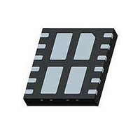
FDMQ8203 Fairchild Semiconductor, FDMQ8203 Datasheet

FDMQ8203
Specifications of FDMQ8203
Related parts for FDMQ8203
FDMQ8203 Summary of contents
Page 1
... Thermal Resistance, Junction to Ambient θJA R Thermal Resistance, Junction to Ambient θJA Package Marking and Ordering Information Device Marking Device FDMQ8203 FDMQ8203 ©2011 Fairchild Semiconductor Corporation FDMQ8203 Rev.C1 General Description This quad mosfet solution provides ten-fold improvement in power dissipation over diode bridge 2 -2 Application = -2 ...
Page 2
... Fall Time f Q Total Gate Charge g Q Total Gate Charge g Q Gate to Source Gate Charge gs Q Gate to Drain “Miller” Charge gd ©2011 Fairchild Semiconductor Corporation FDMQ8203 Rev. °C unless otherwise noted J Test Conditions = 250 μ -250 μ 250 μA, referenced to 25 °C ...
Page 3
... Source to Drain Diode Forward Voltage SD t Reverse Recovery Time rr Q Reverse Recovery Charge rr Notes determined with the device mounted θJA by the user's board design. 2: Pulse Test: Pulse Width < 300 μs, Duty cycle < 2.0%. ©2011 Fairchild Semiconductor Corporation FDMQ8203 Rev. °C unless otherwise noted J Test Conditions -2 ...
Page 4
... JUNCTION TEMPERATURE ( , T J Figure 3. Normalized On Resistance vs Junction Temperature 12 μ PULSE DURATION = 80 s DUTY CYCLE = 0.5% MAX GATE TO SOURCE VOLTAGE (V) GS Figure 5. Transfer Characteristics ©2011 Fairchild Semiconductor Corporation FDMQ8203 Rev. °C unless otherwise noted μ 100 125 150 150 - ...
Page 5
... THIS AREA IS LIMITED BY r DS(on) 0.1 SINGLE PULSE T = MAX RATED 160 C/W θ 0. 0.005 0 DRAIN to SOURCE VOLTAGE (V) DS Figure 9. Forward Bias Safe Operating Area ©2011 Fairchild Semiconductor Corporation FDMQ8203 Rev. °C unless otherwise noted J 1000 100 2.0 2.5 3 100 100 300 MHz V ...
Page 6
... JUNCTION TEMPERATURE ( , T J Figure 12. Normalized On-Resistance vs Junction Temperature 10 μ PULSE DURATION = 80 s DUTY CYCLE = 0.5% MAX 150 GATE TO SOURCE VOLTAGE (V) GS Figure 14. Transfer Characteristics ©2011 Fairchild Semiconductor Corporation FDMQ8203 Rev. unlenss otherwise noted -3 μ -2 Figure 11. Normalized on-Resistance vs Drain 50 75 100 125 150 -55 ...
Page 7
... THIS AREA IS LIMITED BY r DS(on) 0.1 SINGLE PULSE T = MAX RATED 160 C/W θ 0. 0.005 0 DRAIN to SOURCE VOLTAGE (V) DS Figure 18. Forward Bias Safe Operating Area ©2011 Fairchild Semiconductor Corporation FDMQ8203 Rev. unlenss otherwise noted J 1000 100 100 300 7 100 MHz 0.1 ...
Page 8
... Figure 19. Single Pulse Maximum Power Dissipation 2 DUTY CYCLE-DESCENDING ORDER 0.5 0.2 0.1 0.1 0.05 0.02 0.01 0.01 0.001 0.0005 - Figure 20. Junction-to-Ambient Transient Thermal Response Curve ©2011 Fairchild Semiconductor Corporation FDMQ8203 Rev. unlenss otherwise noted PULSE WIDTH (sec) SINGLE PULSE 160 C/W θ ...
Page 9
... Dimensional Outline and Pad Layout ©2011 Fairchild Semiconductor Corporation FDMQ8203 Rev.C1 9 www.fairchildsemi.com ...
Page 10
... Definition of Terms Datasheet Identification Product Status Advance Information Formative / In Design Preliminary First Production No Identification Needed Full Production Obsolete Not In Production ©2011 Fairchild Semiconductor Corporation FDMQ8203 Rev.C1 ® tm ® PowerTrench SM PowerXS™ Programmable Active Droop™ ® QFET QS™ Quiet Series™ ...


