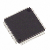
DS21354L Maxim Integrated Products, DS21354L Datasheet - Page 34

DS21354L
Manufacturer Part Number
DS21354L
Description
IC TXRX E1 1-CHIP 3.3V 100-LQFP
Manufacturer
Maxim Integrated Products
Datasheet
1.DS2154LNA2.pdf
(124 pages)
Specifications of DS21354L
Function
Single-Chip Transceiver
Interface
E1, HDLC
Number Of Circuits
1
Voltage - Supply
3.14 V ~ 3.47 V
Current - Supply
75mA
Operating Temperature
0°C ~ 70°C
Mounting Type
Surface Mount
Package / Case
100-LQFP
Includes
Remote and AIS Alarm Detector / Generator
Lead Free Status / RoHS Status
Contains lead / RoHS non-compliant
Power (watts)
-
Available stocks
Company
Part Number
Manufacturer
Quantity
Price
Company:
Part Number:
DS21354L
Manufacturer:
Maxim
Quantity:
241
Company:
Part Number:
DS21354L+
Manufacturer:
TI
Quantity:
2 487
Company:
Part Number:
DS21354LB+
Manufacturer:
Maxim
Quantity:
154
Company:
Part Number:
DS21354LC1+
Manufacturer:
Maxim
Quantity:
90
Company:
Part Number:
DS21354LC1+
Manufacturer:
MAXIM
Quantity:
8
Company:
Part Number:
DS21354LC1+
Manufacturer:
Maxim Integrated
Quantity:
10 000
Part Number:
DS21354LC1+
Manufacturer:
MAXIM/美信
Quantity:
20 000
TCR1: TRANSMIT CONTROL REGISTER 1 (Address = 12 Hex)
(MSB)
Note: See
operation of the DS21354/DS21554.
SYMBOL
ODF
TUA1
TSA1
TFPT
T16S
TSIO
ODF
TSiS
TSM
Figure 18-15
POSITION
TFPT
TCR1.3
TCR1.7
TCR1.6
TCR1.5
TCR1.4
TCR1.2
TCR1.1
TCR1.0
for more details about how the Transmit Control Registers affect the
T16S
Output Data Format.
0 = bipolar data at TPOSO and TNEGO
1 = NRZ data at TPOSO; TNEGO=0
Transmit Time Slot 0 Pass Through.
0 = FAS bits/Sa bits/Remote Alarm sourced internally from the TAF and
TNAF registers
1 = FAS bits/Sa bits/Remote Alarm sourced from TSER
Transmit Time slot 16 Data Select.
0 = sample time slot 16 at TSER pin
1 = source time slot 16 from TS0 to TS15 registers
Transmit Unframed All Ones.
0 = transmit data normally
1 = transmit an unframed all one’s code at TPOSO and TNEGO
Transmit International Bit Select.
0 = sample Si bits at TSER pin
1 = source Si bits from TAF and TNAF registers (in this mode, TCR1.6
must be set to 0)
Transmit Signaling All Ones.
0 = normal operation
1 = force time slot 16 in every frame to all ones
TSYNC Mode Select.
0 = frame mode (see the timing in Section 18.2)
1 = CAS and CRC4 multiframe mode (see the timing in Section 18.2)
TSYNC I/O Select.
0 = TSYNC is an input
1 = TSYNC is an output
TUA1
34 of 124
NAME AND DESCRIPTION
TSiS
TSA1
TSM
(LSB)
TSIO


