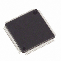
DS21354L Maxim Integrated Products, DS21354L Datasheet - Page 42

DS21354L
Manufacturer Part Number
DS21354L
Description
IC TXRX E1 1-CHIP 3.3V 100-LQFP
Manufacturer
Maxim Integrated Products
Datasheet
1.DS2154LNA2.pdf
(124 pages)
Specifications of DS21354L
Function
Single-Chip Transceiver
Interface
E1, HDLC
Number Of Circuits
1
Voltage - Supply
3.14 V ~ 3.47 V
Current - Supply
75mA
Operating Temperature
0°C ~ 70°C
Mounting Type
Surface Mount
Package / Case
100-LQFP
Includes
Remote and AIS Alarm Detector / Generator
Lead Free Status / RoHS Status
Contains lead / RoHS non-compliant
Power (watts)
-
Available stocks
Company
Part Number
Manufacturer
Quantity
Price
Company:
Part Number:
DS21354L
Manufacturer:
Maxim
Quantity:
241
Company:
Part Number:
DS21354L+
Manufacturer:
TI
Quantity:
2 487
Company:
Part Number:
DS21354LB+
Manufacturer:
Maxim
Quantity:
154
Company:
Part Number:
DS21354LC1+
Manufacturer:
Maxim
Quantity:
90
Company:
Part Number:
DS21354LC1+
Manufacturer:
MAXIM
Quantity:
8
Company:
Part Number:
DS21354LC1+
Manufacturer:
Maxim Integrated
Quantity:
10 000
Part Number:
DS21354LC1+
Manufacturer:
MAXIM/美信
Quantity:
20 000
CCR6: COMMON CONTROL REGISTER 6 (Address = 1D Hex)
LIUODO
TCLKSRC
SYMBOL
LIUODO
(MSB)
LIUSI
RESR
TESR
CDIG
—
—
POSITION
CDIG
CCR6.7
CCR6.6
CCR6.5
CCR6.4
CCR6.3
CCR6.2
CCR6.1
CCR6.0
LIUSI
Line Interface Open-Drain Option. This control bit determines whether
the TTIP and TRING outputs will be open drain or not. The line driver
outputs can be forced open drain to allow 6Vpeak pulses to be generated
or to allow the creation of a very low power interface.
0 = allow TTIP and TRING to operate normally
1 = force the TTIP and TRING outputs to be open drain
Customer Disconnect Indication Generator. This control bit
determines whether the Line Interface will generate an unframed
...1010... pattern at TTIP and TRING instead of the normal data pattern.
0 = generate normal data at TTIP and TRING as input via TPOSI and
TNEGI
1 = generates a ...1010... pattern at TTIP and TRING
Line Interface G.703 Synchronization Interface Enable. This control
bit determines whether the line receiver should handle a normal E1 signal
(Section 6 of G.703) or a 2.048MHz synchronization signal (Section 10
of G.703). This control has no affect on the line interface transmitter.
0 = line receiver configured to support a normal E1 signal
1 = line receiver configured to support a synchronization signal
Not Assigned. Should be set to zero when written.
Not Assigned. Should be set to zero when written.
Transmit Clock Source Select. This function allows the user to
internally select RCLK as the clock source for the transmit-side
formatter.
0 = Source of transmit clock determined by CCR2.2 (LOTCMC)
1 = Force transmitter to internally switch to RCLK as source of transmit
clock. Signal at TCLK pin is ignored
Receive Elastic Store Reset. Setting this bit from a zero to a one will
force the receive elastic store to a depth of one frame. Receive data is lost
during the reset. Should be toggled after RSYSCLK has been applied and
is stable. Must be cleared and set again for a subsequent reset.
Transmit Elastic Store Reset. Setting this bit from a zero to a one will
force the transmit elastic store to a depth of one frame. Transmit data is
lost during the reset. Should be toggled after TSYSCLK has been applied
and is stable. Must be cleared and set again for a subsequent reset.
—
42 of 124
NAME AND DESCRIPTION
—
TCLKSRC
RESR
(LSB)
TESR


