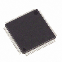
DS21354L Maxim Integrated Products, DS21354L Datasheet - Page 59

DS21354L
Manufacturer Part Number
DS21354L
Description
IC TXRX E1 1-CHIP 3.3V 100-LQFP
Manufacturer
Maxim Integrated Products
Datasheet
1.DS2154LNA2.pdf
(124 pages)
Specifications of DS21354L
Function
Single-Chip Transceiver
Interface
E1, HDLC
Number Of Circuits
1
Voltage - Supply
3.14 V ~ 3.47 V
Current - Supply
75mA
Operating Temperature
0°C ~ 70°C
Mounting Type
Surface Mount
Package / Case
100-LQFP
Includes
Remote and AIS Alarm Detector / Generator
Lead Free Status / RoHS Status
Contains lead / RoHS non-compliant
Power (watts)
-
Available stocks
Company
Part Number
Manufacturer
Quantity
Price
Company:
Part Number:
DS21354L
Manufacturer:
Maxim
Quantity:
241
Company:
Part Number:
DS21354L+
Manufacturer:
TI
Quantity:
2 487
Company:
Part Number:
DS21354LB+
Manufacturer:
Maxim
Quantity:
154
Company:
Part Number:
DS21354LC1+
Manufacturer:
Maxim
Quantity:
90
Company:
Part Number:
DS21354LC1+
Manufacturer:
MAXIM
Quantity:
8
Company:
Part Number:
DS21354LC1+
Manufacturer:
Maxim Integrated
Quantity:
10 000
Part Number:
DS21354LC1+
Manufacturer:
MAXIM/美信
Quantity:
20 000
9.2.2.
Via the THSE control bit (CCR3.2), the DS21354/DS21554 can be set up to take the signaling data
presented at the TSIG pin and insert the signaling data into the PCM data stream that is being input at the
TSER pin. The hardware signaling insertion capabilities of each framer are available whether the
transmit-side elastic store is enabled or disabled. If the transmit-side elastic store is enabled, the
backplane clock (TSYSCLK) must be 2.048MHz/4.096MHz/8.192MHz.
When hardware signaling insertion is enabled on a framer (THSE = 1), then the user must enable the
Transmit Channel Blocking Register Function Select (TCBFS) control bit (CCR3.6 = 1). This is needed
so that the CAS multiframe alignment word, multiframe remote alarm, and spare bits can be added to
time slot 16 in frame 0 of the multiframe. The TS1 register should be programmed with the proper
information. If CCR3.6 = 1, then a zero in the TCBRs implies that signaling data is to be sourced from
TSER (or TSIG if CCR3.2 = 1) and a one implies that signaling data for that channel is to be sourced
from the Transmit Signaling (TS) registers. See definition below.
TCBR1/TCBR2/TCBR3/TCBR4: DEFINITION WHEN CCR3.6 = 1
(MSB)
*These bits should be set to one to allow the internal TS1 register to create the CAS Multiframe Alignment Word and Spare/Remote Alarm bits.
The user can also take advantage of this functionality to intermix signaling data from the TSIG pin and
from the internal Transmit Signaling Registers (TS1 to TS16). As an example, assume that the user
wishes to source all the signaling data except for voice channels 5 and 10 from the TSIG pin. In this
application, the following bits and registers would be programmed as follows:
THSE = 1 (CCR3.2)
TCBFS = 1 (CCR3.6)
T16S = 0 (TCR1.5)
CH18
CH22
CH26
CH30
CONTROL BITS
Transmit Side
CH11
CH15
CH3
CH7
CH17
CH21
CH25
CH29
TS1 = 0Bh (MF alignment word, remote alarm etc.)
TCBR1 = 03h (source time slot 16, frame 1 data)
TCBR2 = 01h (source voice Channel 5 signaling data from TS6)
CBR3 = 04h (source voice Channel 10 signaling data from TS11)
TCBR4 = 00h
CH10
CH14
CH2
CH6
CH16
CH20
CH24
CH28
59 of 124
DS21354/DS21554 3.3V/5V E1 Single-Chip Transceivers
REGISTER VALUES
CH13
CH1
CH5
CH9
CH19
CH23
CH27
1*
(LSB)
CH12
CH4
CH8
1*
TCBR1(22)
TCBR2(23)
TCBR3(24)
TCBR4(25)


