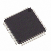
DS21354L Maxim Integrated Products, DS21354L Datasheet - Page 81

DS21354L
Manufacturer Part Number
DS21354L
Description
IC TXRX E1 1-CHIP 3.3V 100-LQFP
Manufacturer
Maxim Integrated Products
Datasheet
1.DS2154LNA2.pdf
(124 pages)
Specifications of DS21354L
Function
Single-Chip Transceiver
Interface
E1, HDLC
Number Of Circuits
1
Voltage - Supply
3.14 V ~ 3.47 V
Current - Supply
75mA
Operating Temperature
0°C ~ 70°C
Mounting Type
Surface Mount
Package / Case
100-LQFP
Includes
Remote and AIS Alarm Detector / Generator
Lead Free Status / RoHS Status
Contains lead / RoHS non-compliant
Power (watts)
-
Available stocks
Company
Part Number
Manufacturer
Quantity
Price
Company:
Part Number:
DS21354L
Manufacturer:
Maxim
Quantity:
241
Company:
Part Number:
DS21354L+
Manufacturer:
TI
Quantity:
2 487
Company:
Part Number:
DS21354LB+
Manufacturer:
Maxim
Quantity:
154
Company:
Part Number:
DS21354LC1+
Manufacturer:
Maxim
Quantity:
90
Company:
Part Number:
DS21354LC1+
Manufacturer:
MAXIM
Quantity:
8
Company:
Part Number:
DS21354LC1+
Manufacturer:
Maxim Integrated
Quantity:
10 000
Part Number:
DS21354LC1+
Manufacturer:
MAXIM/美信
Quantity:
20 000
15.1.
The DS21354/DS21554 contain a digital clock recovery system. See
details. The device couples to the receive-E1-shielded twisted pair or coax via a 1:1 transformer. See
Table 15-3
multiplied by 16 via an internal PLL and fed to the clock recovery system. The clock recovery system
uses the clock from the PLL circuit to form a 16-times oversampler, which is used to recover the clock
and data. This oversampling technique offers outstanding jitter tolerance
Normally, the clock that is output at the RCLKO pin is the recovered clock from the E1 AMI/HDB3
waveform presented at the RTIP and RRING inputs. When no AMI signal is present at RTIP and RRING,
a receive carrier loss (RCL) condition occurs, and the RCLKO is sourced from the clock applied at the
MCLK pin. If the jitter attenuator is either placed in the transmit path or is disabled, the RCLKO output
can exhibit slightly shorter high cycles of the clock, which is due to the highly oversampled digital clock
recovery circuitry. If the jitter attenuator is placed in the receive path (as is the case in most applications),
the jitter attenuator restores the RCLK to being close to 50% duty cycle. Please see the Receive AC
Timing Characteristics for more details.
15.2.
The DS21354/DS21554 use a set of laser-trimmed delay lines along with a precision digital-to-analog
converter (DAC) to create the waveforms that are transmitted onto the E1 line. The waveforms meet the
ITU G.703 specifications (see
The user selects which waveform is to be generated by properly programming the L2/L1/L0 bits in the
Line Interface Control Register (LICR). The DS21354/DS21554 can set up in a number of various
configurations depending on the application. See tables below and
Table 15-1. Line Build-Out Select in LICR for the DS21554
* N.M. = Not Meaningful (return loss value too low for significance).
** Refer to Application Note 324 for details on E1 line interface design.
L2
0
0
0
0
1
1
1
L1
0
0
1
1
0
1
0
Receive Clock and Data Recovery
Transmit Waveshaping and Line Driving
L0
0
1
0
1
0
0
0
for transformer details. The 2.048MHz clock attached at the MCLK pin is internally
120W with protection resistors
75W with protection resistors
120W with high return loss
75W with high return loss
75W with high return loss
APPLICATION
120W normal
75W normal
Figure
15-5).
81 of 124
TRANSFORMER
1:1.15 step-up
1:1.15 step-up
1:1.15 step-up
1:1.15 step-up
1:1.15 step-up
1:1.36 step-up
1:1.36 step-up
Figure
Figure 2-1
(Figure
RETURN LOSS
15-5.
(dB)
N.M.
N.M.
N.M.
N.M.
21
21
21
and
15-3).
*
Figure 15-1
RT (W)
8.2
8.2
27
18
27
0
0
for more
**


