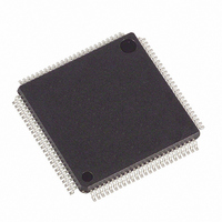
DS21354L Maxim Integrated Products, DS21354L Datasheet - Page 82

DS21354L
Manufacturer Part Number
DS21354L
Description
IC TXRX E1 1-CHIP 3.3V 100-LQFP
Manufacturer
Maxim Integrated Products
Datasheet
1.DS2154LNA2.pdf
(124 pages)
Specifications of DS21354L
Function
Single-Chip Transceiver
Interface
E1, HDLC
Number Of Circuits
1
Voltage - Supply
3.14 V ~ 3.47 V
Current - Supply
75mA
Operating Temperature
0°C ~ 70°C
Mounting Type
Surface Mount
Package / Case
100-LQFP
Includes
Remote and AIS Alarm Detector / Generator
Lead Free Status / RoHS Status
Contains lead / RoHS non-compliant
Power (watts)
-
Available stocks
Company
Part Number
Manufacturer
Quantity
Price
Company:
Part Number:
DS21354L
Manufacturer:
Maxim
Quantity:
241
Company:
Part Number:
DS21354L+
Manufacturer:
TI
Quantity:
2 487
Company:
Part Number:
DS21354LB+
Manufacturer:
Maxim
Quantity:
154
Company:
Part Number:
DS21354LC1+
Manufacturer:
Maxim
Quantity:
90
Company:
Part Number:
DS21354LC1+
Manufacturer:
MAXIM
Quantity:
8
Company:
Part Number:
DS21354LC1+
Manufacturer:
Maxim Integrated
Quantity:
10 000
Part Number:
DS21354LC1+
Manufacturer:
MAXIM/美信
Quantity:
20 000
Table 15-2. Line Build-Out Select in LICR for the DS21354
* N.M. = Not Meaningful (return loss value too low for significance).
** Refer to Application Note 324 for details on E1 line interface design.
Due to the nature of the design of the transmitter in the DS21354/DS21554, very little jitter (less than
0.005 UI
created is independent of the duty cycle of TCLK. The transmitter in the device couples to the E1-
transmit-shielded twisted pair or coax via a 1:1.15 or 1:1.36 step-up transformer as shown in
For the devices to create the proper waveforms, the transformer used must meet the specifications listed
in
(RMS) from being sourced in a 1W load.
Table 15-3. Transformer Specifications
Turns Ratio for DS21354
Turns Ratio for DS21554
Primary Inductance
Leakage Inductance
Intertwining Capacitance
DC Resistance
15.3.
The DS21354/DS21554 contain an on-board jitter attenuator that can be set to a depth of either 32 or 128
bits via the JABDS bit in the Line Interface Control Register (LICR). The 128-bit mode is used in
applications where large excursions of wander are expected. The 32-bit mode is used in delay-sensitive
applications. The characteristics of the attenuation are shown in
placed in either the receive path or the transmit path by appropriately setting or clearing the JAS bit in the
LICR. Also, the jitter attenuator can be disabled (in effect, removed) by setting the DJA bit in the LICR.
For the jitter attenuator to properly operate, a 2.048MHz clock (±50ppm) must be applied at the MCLK
pin, or a crystal with similar characteristics must be applied across the MCLK and XTALD pins. If a
crystal is applied across the MCLK and XTALD pins, then the maximum effective series resistance
should be 30W, and capacitors should be placed from each leg of the crystal to ground as shown in
Figure
the clock applied at the TCLKI pin to create a smooth jitter-free clock, which is used to clock data out of
the jitter attenuator FIFO. It is acceptable to provide a gapped/bursty clock at the TCLKI pin if the jitter
attenuator is placed on the transmit side. If the incoming jitter exceeds either 120 UI
128 bits) or 28 UI
32.768MHz clock by either 15 or 17 instead of the normal 16 to keep the buffer from overflowing. When
the device divides by either 15 or 17, it also sets the Jitter Attenuator Limit Trip (JALT) bit in the Receive
Information Register (RIR.5).
L2
0
0
0
0
1
1
Table
L1
0
0
1
1
0
0
15-2. On-board circuitry adjusts either the recovered clock from the clock/data recovery block or
Jitter Attenuator
P-P
15-3. The line driver in the device contains a current limiter that prevents more than 50mA
L0
broadband from 10Hz to 100kHz) is added to the jitter present on TCLK. Also, the waveform
0
1
0
1
0
1
SPECIFICATION
120W with protection resistors
75W with protection resistors
P-P
120W with high return loss
75W with high return loss
(buffer depth is 32 bits), then the DS21354/DS21554 divide the internal nominal
APPLICATION
120W normal
75W normal
82 of 124
TRANSFORMER
1:2 step-up
1:2 step-up
1:2 step-up
1:2 step-up
1:2 step-up
1:2 step-up
1:1 (receive) and 1:2 (transmit) ±3%
1:1 (receive) and 1:1.15 or 1:1.36 (transmit) ±3%
600mH minimum
1.0mH maximum
40pF maximum
1.2W maximum
RECOMMENDED VALUE
Figure
RETURN LOSS (dB)
15-4. The jitter attenuator can be
N.M.
N.M.
N.M.
N.M.
21
21
P-P
(buffer depth is
*
Figure
RT (W)
11.6
2.5
2.5
6.2
0
0
15-1.
**


