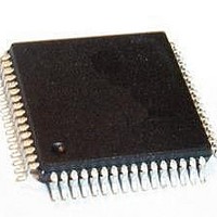
PSB 2132 H V2.2 Infineon Technologies, PSB 2132 H V2.2 Datasheet - Page 36

PSB 2132 H V2.2
Manufacturer Part Number
PSB 2132 H V2.2
Description
IC CODEC FILTER 2CHAN MQFP-64
Manufacturer
Infineon Technologies
Series
SICOFI®r
Datasheet
1.PSB_2132_H_V2.2.pdf
(69 pages)
Specifications of PSB 2132 H V2.2
Package / Case
64-QFP
Function
CODEC Filter
Interface
IOM-2 PCM, SPI
Number Of Circuits
2
Voltage - Supply
5V
Current - Supply
18mA
Power (watts)
90mW
Mounting Type
Surface Mount
Includes
Level Metering Function, Tone Generation
Number Of Adc Inputs
2
Number Of Dac Outputs
2
Interface Type
Serial
Operating Supply Voltage
5 V
Maximum Operating Temperature
+ 70 C
Mounting Style
SMD/SMT
Minimum Operating Temperature
0 C
Number Of Channels
2
Snr
35.4 dB
Supply Current
40 mA
Lead Free Status / RoHS Status
Lead free / RoHS Compliant
Operating Temperature
-
Lead Free Status / RoHS Status
Lead free / RoHS Compliant, Lead free / RoHS Compliant
Other names
PSB2132HV2.2XT
SP000007696
SP000007696
Hardware Reference Manual
5.1.2
Table 21
5.2
The SICOFI
interface in terminal mode (3 IOM channels, 768 kbit/s). The device uses the IOM-clock
DCL at 1536 kHz as a master clock. The bit clock input BCL can be at either 768 kHz or
1536 kHz. FCS is an 8 kHz input. The SICOFI
output Pin 26 assigned to the IOM Data Upstream signal, DU. Further, input Pin 27 and
output Pin 29 are assigned to the IOM Data Downstream signal, DD. This configuration
allows transmission and reception of PCM data on either DU or DD. It further enables
internal connections of channels, by programming the receive time slot of one channel
to the transmit time slot of the other channel, and vice versa.
The IOM-2 PCM Interface has the following characteristics and features:
• Data rate of 768 kbit/s,
• Bit clock input (BCL) configurable for 768 kHz or 1536 kHz,
• IOM-2 DCL signal used as 1536 kHz master clock for the device; must be applied for
• 12 time slots per IOM-2 frame,
• PCM data format serialized 8 bits with MSB first,
• Configurable A-Law or µ-Law coding,
• Independent time slot assignment for each channel and direction,
• Internal voice connection between channels possible,
• Programmable sampling slopes,
• Programmable frame delay.
Symbol
GNDA1
GNDA2
V
V
V
V
all device functions,
V
V
V
DDREF
DDA12
OUT1
OUT2
REF
IN1
IN2
Analog Interface Pins
IOM-2 PCM Interface
Pin
®
49
55
51
53
50
54
52
57
56
2-TE’s IOM-2 PCM Interface can be connected directly to an IOM-2
Analog Interface Pins
Analog Input, Channel 1, 2
Requires a coupling capacitor >39 nF to the SLIC, see Figure 14.
Analog Output, Channel 1, 2
Requires a coupling capacitor to the SLIC. The capacitor’s value
depends on the input impedance of the SLIC, see Figure 14.
Analog Ground, Channel 1, 2
Not internally connected to GNDD or the other GNDAx.
Analog Supply Voltage, Channels 1+2
+5 V (100 nF blocking capacitor required, see Figure 14).
Analog Supply Reference Voltage,
+5 V (100 nF blocking capacitor required, see Figure 14).
Reference Voltage
Must connect to a 220 nF cap. to ground, see Figure 14.
27
Function
®
2-TE has data input Pin 30 and data
Interface Description
PSB 2132
2001-02-20


