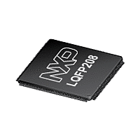
LPC2939 NXP Semiconductors, LPC2939 Datasheet - Page 14

LPC2939
Manufacturer Part Number
LPC2939
Description
The LPC2939 combine an ARM968E-S CPU core with two integrated TCM blocksoperating at frequencies of up to 125 MHz, Full-speed USB 2
Manufacturer
NXP Semiconductors
Datasheet
1.LPC2939.pdf
(99 pages)
Available stocks
Company
Part Number
Manufacturer
Quantity
Price
Company:
Part Number:
LPC2939FBD208
Manufacturer:
NXP
Quantity:
105 000
Company:
Part Number:
LPC2939FBD208,551
Manufacturer:
NXP Semiconductors
Quantity:
10 000
Company:
Part Number:
LPC2939FET208,551
Manufacturer:
NXP Semiconductors
Quantity:
10 000
NXP Semiconductors
6. Functional description
LPC2939_3
Product data sheet
6.1 Architectural overview
6.2 ARM968E-S processor
The LPC2939 consists of:
The LPC2939 configures the ARM968E-S processor in little-endian byte order. All
peripherals run at their own clock frequency to optimize the total system power
consumption. The AHB-to-APB bridge used in the subsystems contains a write-ahead
buffer one transaction deep. This implies that when the ARM968E-S issues a buffered
write action to a register located on the APB side of the bridge, it continues even though
the actual write may not yet have taken place. Completion of a second write to the same
subsystem will not be executed until the first write is finished.
The ARM968E-S is a general purpose 32-bit RISC processor, which offers high
performance and very low power consumption. The ARM architecture is based on
Reduced Instruction Set Computer (RISC) principles, and the instruction set and related
decode mechanism are much simpler than those of microprogrammed Complex
Instruction Set Computers (CISC). This simplicity results in a high instruction throughput
and impressive real-time interrupt response from a small and cost-effective controller
core.
Amongst the most compelling features of the ARM968E-S are:
Pipeline techniques are employed so that all parts of the processing and memory systems
can operate continuously. The ARM968E-S is based on the ARMv5TE five-stage pipeline
architecture. Typically, in a three-stage pipeline architecture, while one instruction is being
executed its successor is being decoded and a third instruction is being fetched from
memory. In the five-stage pipeline additional stages are added for memory access and
write-back cycles.
•
•
•
•
•
•
•
•
An ARM968E-S processor with real-time emulation support
An AMBA multilayer Advanced High-performance Bus (AHB) for interfacing to the
on-chip memory controllers
Two DTL buses (an universal NXP interface) for interfacing to the interrupt controller
and the Power, Clock and Reset Control SubSystem (PCRSS)
Three ARM Peripheral Buses (APB - a compatible super set of ARM's AMBA
advanced peripheral bus) for connection to on-chip peripherals clustered in
subsystems
One ARM Peripheral Bus for event router and system control
Separate directly connected instruction and data Tightly Coupled Memory (TCM)
interfaces
Write buffers for the AHB and TCM buses
Enhanced 16 32 multiplier capable of single-cycle MAC operations and 16-bit fixed-
point DSP instructions to accelerate signal-processing algorithms and applications
All information provided in this document is subject to legal disclaimers.
Rev. 03 — 7 April 2010
ARM9 microcontroller with CAN, LIN, and USB
LPC2939
© NXP B.V. 2010. All rights reserved.
14 of 99


