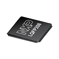
LPC2939 NXP Semiconductors, LPC2939 Datasheet - Page 37

LPC2939
Manufacturer Part Number
LPC2939
Description
The LPC2939 combine an ARM968E-S CPU core with two integrated TCM blocksoperating at frequencies of up to 125 MHz, Full-speed USB 2
Manufacturer
NXP Semiconductors
Datasheet
1.LPC2939.pdf
(99 pages)
Available stocks
Company
Part Number
Manufacturer
Quantity
Price
Company:
Part Number:
LPC2939FBD208
Manufacturer:
NXP
Quantity:
105 000
Company:
Part Number:
LPC2939FBD208,551
Manufacturer:
NXP Semiconductors
Quantity:
10 000
Company:
Part Number:
LPC2939FET208,551
Manufacturer:
NXP Semiconductors
Quantity:
10 000
NXP Semiconductors
LPC2939_3
Product data sheet
6.13.5.2 Pin description
6.13.5.3 Clock description
6.13.6 General-Purpose I/O (GPIO)
The SPI module’s operating mode, frame format, and word size are programmed through
the SLVn_SETTINGS registers.
A single combined interrupt request SPI_INTREQ output is asserted if any of the
interrupts are asserted and unmasked.
Depending on the operating mode selected, the SPI SCS outputs operate as an
active-HIGH frame synchronization output for Texas Instruments synchronous serial
frame format or an active-LOW chip select for SPI.
Each data frame is between four and 16 bits long, depending on the size of words
programmed, and is transmitted starting with the MSB.
The SPI pins are combined with other functions on the port pins of the LPC2939, see
Section
Table 18.
[1]
[2]
The SPI modules are clocked by two different clocks; CLK_SYS_PESS and CLK_SPIx
(x = 0, 1, 2), see
power management. The frequency of all clocks CLK_SPIx is identical as they are derived
from the same base clock BASE_CLK_SPI. The register interface towards the system bus
is clocked by CLK_SYS_PESS. The serial-clock rate divisor is clocked by CLK_SPIx.
The SPI clock frequency can be controlled by the CGU. In master mode the SPI clock
frequency (CLK_SPIx) must be set to at least twice the SPI serial clock rate on the
interface. In slave mode CLK_SPIx must be set to four times the SPI serial clock rate on
the interface.
The LPC2939 contains six general-purpose I/O ports located at different peripheral base
addresses. In the 208-pin package all six ports are available. All I/O pins are bidirectional,
and the direction can be programmed individually. The I/O pad behavior depends on the
configuration programmed in the port function-select registers.
The key features are:
Symbol
SPIx SCSy
SPIx SCK
SPIx SDI
SPIx SDO
•
•
•
Direction of SPIx SCS and SPIx SCK pins depends on master or slave mode. These pins are output in
master mode, input in slave mode.
In slave mode there is only one chip select input pin, SPIx SCS0. The other chip selects have no function in
slave mode.
General-purpose parallel inputs and outputs
Direction control of individual bits
Synchronized input sampling for stable input data values
6.12.3.
SPI pins
Pin name
SCSx[y]
SCKx
SDIx
SDOx
All information provided in this document is subject to legal disclaimers.
Table 18
Section
Rev. 03 — 7 April 2010
6.7.2. Note that each SPI has its own CLK_SPIx branch clock for
shows the SPI pins (x runs from 0 to 2; y runs from 0 to 3).
Direction
IN/OUT
IN/OUT
IN
OUT
ARM9 microcontroller with CAN, LIN, and USB
Description
SPIx chip select
SPIx clock
SPIx data input
SPIx data output
[1]
[1][2]
LPC2939
© NXP B.V. 2010. All rights reserved.
37 of 99


