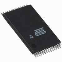
AT45DB642D-TU Atmel, AT45DB642D-TU Datasheet - Page 25

AT45DB642D-TU
Manufacturer Part Number
AT45DB642D-TU
Description
IC FLASH 64MBIT 66MHZ 28TSOP
Manufacturer
Atmel
Datasheet
1.AT45DB642D-CU.pdf
(58 pages)
Specifications of AT45DB642D-TU
Format - Memory
FLASH
Memory Type
DataFLASH
Memory Size
64M (8192 pages x 1056 bytes)
Speed
66MHz
Interface
Parallel/Serial
Voltage - Supply
2.7 V ~ 3.6 V
Operating Temperature
-40°C ~ 85°C
Package / Case
28-TSOP
Density
64Mb
Access Time (max)
6ns
Interface Type
Parallel/Serial-SPI
Boot Type
Not Required
Address Bus
1/8Bit
Operating Supply Voltage (typ)
3.3V
Operating Temp Range
-40C to 85C
Package Type
TSOP-I
Program/erase Volt (typ)
2.7 to 3.6V
Sync/async
Synchronous
Operating Temperature Classification
Industrial
Operating Supply Voltage (min)
2.7V
Operating Supply Voltage (max)
3.6V
Word Size
8b
Number Of Words
8M
Supply Current
15mA
Mounting
Surface Mount
Pin Count
28
Data Bus Width
8 bit
Architecture
Sectored
Supply Voltage (max)
3.6 V
Supply Voltage (min)
2.7 V
Maximum Operating Current
15 mA
Mounting Style
SMD/SMT
Organization
256 KB x 32
Memory Configuration
8192 Pages X 1056 Bytes
Clock Frequency
66MHz
Supply Voltage Range
2.7V To 3.6V
Memory Case Style
TSOP
Rohs Compliant
Yes
Lead Free Status / RoHS Status
Lead free / RoHS Compliant
Available stocks
Company
Part Number
Manufacturer
Quantity
Price
Company:
Part Number:
AT45DB642D-TU
Manufacturer:
MICRON
Quantity:
101
Company:
Part Number:
AT45DB642D-TU
Manufacturer:
ATMEL
Quantity:
9 396
Company:
Part Number:
AT45DB642D-TU
Manufacturer:
AT
Quantity:
5
Part Number:
AT45DB642D-TU
Manufacturer:
ATMEL/爱特梅尔
Quantity:
20 000
13. “Power of 2” Binary Page Size Option
13.1
14. Manufacturer and Device ID Read
3542K–DFLASH–04/09
Programming the Configuration Register
“Power of 2” binary page size Configuration Register is a user-programmable nonvolatile regis-
ter that allows the page size of the main memory to be configured for binary page size
(1024 bytes) or standard DataFlash page size (1056 bytes). The “power of 2” page size is a
one-time programmable configuration register and once the device is configured for
“power of 2” page size, it cannot be reconfigured again. The devices are initially shipped
with the page size set to 1056 bytes. The user has the option of ordering binary page size (1024
bytes) devices from the factory. For details, please refer to
page
For the binary “power of 2” page size to become effective, the following steps must be followed:
If the above steps are not followed in setting the the page size prior to page programming, user
may expect incorrect data during a read operation.
To program the Configuration Register for “power of 2” binary page size, the CS pin must first be
asserted as it would be with any other command. Once the CS pin has been asserted, the
appropriate 4-byte opcode sequence must be clocked into the device in the correct order. The 4-
byte opcode sequence must start with 3DH and be followed by 2AH, 80H, and A6H. After the
last bit of the opcode sequence has been clocked in, the CS pin must be deasserted to initiate
the internally self-timed program cycle. The programming of the Configuration Register should
take place in a time of t
busy. The device must be power-cycled after the completion of the program cycle to set the
“power of 2” page size. If the device is powered-down before the completion of the program
cycle, then setting the Configuration Register cannot be guaranteed. However, the user should
check bit 0 of the status register to see whether the page size was configured for binary page
size. If not, the command can be re-issued again.
Figure 13-1. Erase Sector Protection Register
Identification information can be read from the device to enable systems to electronically query
and identify the device while it is in system. The identification method and the command opcode
comply with the JEDEC standard for “Manufacturer and Device ID Read Methodology for SPI
Compatible Serial Interface Memory Devices”. The type of information that can be read from the
Command
Power of Two Page Size
1. Program the one-time programmable configuration resister using opcode sequence
2. Power cycle the device (i.e. power down and power up again).
3. User can now program the page for the binary page size.
51.
3DH, 2AH, 80H and A6H (please see
SI or IO
7
- IO
CS
0
P
, during which time the Status Register will indicate that the device is
Each transition
represents 8 bits
Opcode
Byte 1
Section
Opcode
Byte 2
Byte 1
13.1).
3DH
Opcode
Byte 3
Section 27. ”Ordering Information” on
Byte 2
2AH
Opcode
Byte 4
Byte 3
80H
Byte 4
A6H
25


