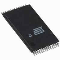
AT45DB642D-TU Atmel, AT45DB642D-TU Datasheet - Page 32

AT45DB642D-TU
Manufacturer Part Number
AT45DB642D-TU
Description
IC FLASH 64MBIT 66MHZ 28TSOP
Manufacturer
Atmel
Datasheet
1.AT45DB642D-CU.pdf
(58 pages)
Specifications of AT45DB642D-TU
Format - Memory
FLASH
Memory Type
DataFLASH
Memory Size
64M (8192 pages x 1056 bytes)
Speed
66MHz
Interface
Parallel/Serial
Voltage - Supply
2.7 V ~ 3.6 V
Operating Temperature
-40°C ~ 85°C
Package / Case
28-TSOP
Density
64Mb
Access Time (max)
6ns
Interface Type
Parallel/Serial-SPI
Boot Type
Not Required
Address Bus
1/8Bit
Operating Supply Voltage (typ)
3.3V
Operating Temp Range
-40C to 85C
Package Type
TSOP-I
Program/erase Volt (typ)
2.7 to 3.6V
Sync/async
Synchronous
Operating Temperature Classification
Industrial
Operating Supply Voltage (min)
2.7V
Operating Supply Voltage (max)
3.6V
Word Size
8b
Number Of Words
8M
Supply Current
15mA
Mounting
Surface Mount
Pin Count
28
Data Bus Width
8 bit
Architecture
Sectored
Supply Voltage (max)
3.6 V
Supply Voltage (min)
2.7 V
Maximum Operating Current
15 mA
Mounting Style
SMD/SMT
Organization
256 KB x 32
Memory Configuration
8192 Pages X 1056 Bytes
Clock Frequency
66MHz
Supply Voltage Range
2.7V To 3.6V
Memory Case Style
TSOP
Rohs Compliant
Yes
Lead Free Status / RoHS Status
Lead free / RoHS Compliant
Available stocks
Company
Part Number
Manufacturer
Quantity
Price
Company:
Part Number:
AT45DB642D-TU
Manufacturer:
MICRON
Quantity:
101
Company:
Part Number:
AT45DB642D-TU
Manufacturer:
ATMEL
Quantity:
9 396
Company:
Part Number:
AT45DB642D-TU
Manufacturer:
AT
Quantity:
5
Part Number:
AT45DB642D-TU
Manufacturer:
ATMEL/爱特梅尔
Quantity:
20 000
16. Power-on/Reset State
16.1
17. System Considerations
32
Initial Power-up/Reset Timing Restrictions
AT45DB642D
When power is first applied to the device, or when recovering from a reset condition, the device
will default to Mode 3. In addition, the output pins (SO or I/O7 - I/O0) will be in a high impedance
state, and a high-to-low transition on the CS pin will be required to start a valid instruction. The
mode (Mode 3 or Mode 0) will be automatically selected on every falling edge of CS by sampling
the inactive clock state.
At power up, the device must not be selected until the supply voltage reaches the V
further delay of t
reset mode until the V
operations are disabled and the device does not respond to any commands. After power up is
applied and the V
before the device can be selected in order to perform a read operation.
Similarly, the t
value (V
power-up, the device will default in Standby mode.
The RapidS serial interface is controlled by the clock SCK, serial input SI and chip select CS
pins. The sequential 8-bit Rapid8 is controlled by the clock CLK, 8 I/Os and chip select CS pins.
These signals must rise and fall monotonically and be free from noise. Excessive noise or ring-
ing on these pins can be misinterpreted as multiple edges and cause improper operation of the
device. The PC board traces must be kept to a minimum distance or appropriately terminated to
ensure proper operation. If necessary, decoupling capacitors can be added on these pins to pro-
vide filtering against noise glitches.
As system complexity continues to increase, voltage regulation is becoming more important. A
key element of any voltage regulation scheme is its current sourcing capability. Like all Flash
memories, the peak current for DataFlash occur during the programming and erase operation.
The regulator needs to supply this peak current requirement. An under specified regulator can
cause current starvation. Besides increasing system noise, current starvation during program-
ming or erase can lead to improper operation and possible data corruption.
The device uses an adaptive algorithm during program and erase operations. In order to opti-
mize the erase and program time, use the RDY/BUSY bit of the status register or the
RDY/BUSY pin to determine whether the program or erase operation was completed. Fixed tim-
ing is not recommended.
Symbol
t
t
V
VCSL
PUW
POR
POR
) before the device can perform a write (Program or Erase) operation. After initial
Parameter
V
Power-Up Device Delay before Write
allowed
Power-ON Reset Voltage
PUW
CC
VCSL
CC
(min.) to Chip Select low
delay is required after the V
. During power-up, the internal Power-on Reset circuitry keeps the device in
is at the minimum operating voltage V
CC
rises above the Power-on Reset threshold value (V
CC
rises above the Power-on Reset threshold
Min
1.5
50
CC
(min.), the t
Typ
VCSL
POR
Max
2.5
20
delay is required
3542K–DFLASH–04/09
). At this time, all
CC
(min.) and
Units
ms
µs
V


