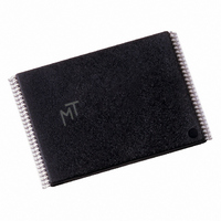
MT28F320J3RG-11 GMET TR Micron Technology Inc, MT28F320J3RG-11 GMET TR Datasheet - Page 11

MT28F320J3RG-11 GMET TR
Manufacturer Part Number
MT28F320J3RG-11 GMET TR
Description
IC FLASH 32MBIT 110NS 56TSOP
Manufacturer
Micron Technology Inc
Datasheet
1.MT28F128J3FS-12_ET_TR.pdf
(55 pages)
Specifications of MT28F320J3RG-11 GMET TR
Format - Memory
FLASH
Memory Type
FLASH
Memory Size
32M (4Mx8, 2Mx16)
Speed
110ns
Interface
Parallel
Voltage - Supply
2.7 V ~ 3.6 V
Operating Temperature
-40°C ~ 85°C
Package / Case
56-TSOP
Lead Free Status / RoHS Status
Contains lead / RoHS non-compliant
Memory Architecture
memory array architecture is divided into one hun-
dred twenty-eight, sixty-four, or thirty-two 128KB
blocks, respectively (see Figure 6). The internal archi-
tecture allows greater flexibility when updating data
because individual code portions can be updated
independently of the rest of the code.
Read
identifier codes, or status register, regardless of the
V
array mode upon initial device power-up or after exit
from reset/power-down mode. To access other read
mode commands (READ ARRAY, READ QUERY, READ
IDENTIFIER CODES, or READ STATUS REGISTER),
these commands should be issued to the CUI. Six con-
trol pins dictate the data flow in and out of the device:
CE0, CE1, CE2, OE#, WE#, and RP#. In system designs
using multiple Q-Flash devices, CE0, CE1, and CE2
(CEx) select the memory device (see Table 2). To drive
data out of the device and onto the I/O bus, OE# must
be active and WE# must be inactive (V
09005aef80b5a323
MT28F640J3.fm – Rev. N 3/05 EN
PEN
The MT28F128J3, MT28F640J3, and MT28F320J3
Information can be read from any block, query,
voltage. The device automatically resets to read
Figure 6: Memory Map
IH
).
11
Table 2:
NOTE:
device defaults to asynchronous page mode, thus pro-
viding a high data transfer rate for memory sub-
systems. In this state, data is internally read and stored
in a high-speed page buffer. A0–A2 select data in the
page buffer. Asynchronous page mode, with a page
size of four words or eight bytes, is supported with no
additional commands required and can be used to
access all blocks. Page mode can be used to access reg-
ister information, but only one word is loaded into the
page buffer.
Output Disable
HIGH level (V
in High-Z.
Standby
Table 2) and place it in standby mode, which substan-
tially reduces device power consumption. DQ0–DQ15
outputs are placed in High-Z, independent of OE#. If
deselected during block erase, program, or lock bit
configuration, the ISM continues functioning and con-
suming active power until the operation completes.
Reset/Power-Down
mode when set to V
places output drivers in High-Z, and turns off internal
circuitry. RP# must be held LOW for a minimum of
t
until initial memory access outputs are valid. After this
PLPH.
For single-chip applications, CE2 and CE1 can be con-
nected to GND.
When reading information in read array mode, the
The device outputs are disabled with OE# at a logic
CE0, CE1, and CE2 can disable the device (see
RP# puts the device into the reset/power-down
During read, RP# LOW deselects the memory,
CE2
V
V
V
V
V
V
V
V
Micron Technology, Inc., reserves the right to change products or specifications without notice.
IH
IH
IH
IH
IL
IL
IL
IL
t
RWH is required after return from reset mode
IH
Chip-Enable Truth Table
). Output pins DQ0–DQ15 are placed
CE1
V
V
V
V
128Mb, 64Mb, 32Mb
V
V
V
V
IL
IH
IH
IH
IH
IL
IL
IL
IL
.
Q-FLASH MEMORY
CE0
V
V
V
V
V
V
V
V
IH
IH
IH
IH
IL
IL
IL
IL
©2000 Micron Technology. Inc.
Disabled
Disabled
Disabled
Disabled
DEVICE
Enabled
Enabled
Enabled
Enabled


