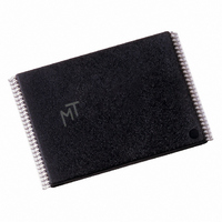
MT28F320J3RG-11 GMET TR Micron Technology Inc, MT28F320J3RG-11 GMET TR Datasheet - Page 39

MT28F320J3RG-11 GMET TR
Manufacturer Part Number
MT28F320J3RG-11 GMET TR
Description
IC FLASH 32MBIT 110NS 56TSOP
Manufacturer
Micron Technology Inc
Datasheet
1.MT28F128J3FS-12_ET_TR.pdf
(55 pages)
Specifications of MT28F320J3RG-11 GMET TR
Format - Memory
FLASH
Memory Type
FLASH
Memory Size
32M (4Mx8, 2Mx16)
Speed
110ns
Interface
Parallel
Voltage - Supply
2.7 V ~ 3.6 V
Operating Temperature
-40°C ~ 85°C
Package / Case
56-TSOP
Lead Free Status / RoHS Status
Contains lead / RoHS non-compliant
Design Considerations
Five-Line Output Control
OE#, and RP#) to accommodate multiple memory
connections in large memory arrays. This control pro-
vides the lowest possible memory power dissipation
and ensures that data bus contention does not occur.
decoder should enable the device (see Table 2 on
page 11) while OE# is connected to all memory devices
and the system’s READ# control line. This ensures that
only selected memory devices have active outputs
while deselected memory devices are in standby
mode. During system power transitions, RP# should
be connected to the system POWERGOOD signal to
prevent unintended writes. POWERGOOD should also
toggle during system reset.
STS and Block Erase, Program, and Lock
Bit Configuration
Polling
to V
method of detecting block erase, program, and lock bit
configuration completion. It is recommended that a
2.5KΩ resistor be used between STS# and V
default mode, it transitions low after block erase, pro-
gram, or lock bit configuration commands and returns
to High-Z when the ISM has finished executing the
internal algorithm. See the CONFIGURATION com-
mand for alternate configurations of the STS pin. STS
can be connected to an interrupt input of the system
CPU or controller. STS is active at all times. In default
mode, it is also High-Z when the device is in block
erase suspend (with programming inactive), program
suspend, or reset/power-down mode.
Power Supply Decoupling
power switching characteristics. There are three sup-
ply current issues to consider: standby current levels,
active current levels, and transient peaks produced by
falling and rising edges of CEx and OE#. Transient cur-
rent magnitudes depend on the device outputs’ capac-
itive and inductive loading. Two-line control and
proper decoupling capacitor selection suppresses
transient voltage peaks. Because Micron Q-Flash
memory devices draw their power from three V
(these devices do not include a V
09005aef80b5a323
MT28F640J3.fm – Rev. N 3/05 EN
Micron provides five control inputs (CE0, CE1, CE2,
To efficiently use these control inputs, an address
As an open drain output, STS should be connected
Device decoupling is required for Flash memory
CC
Q by a pull-up resistor to provide a hardware
PP
pin), it is recom-
CC
CC
Q. In
pins
39
mended that systems without separate power and
ground planes attach a 0.1µF ceramic capacitor
between each of the device’s three V
includes V
inductance capacitors should be placed as close as
possible to package leads on each Micron Q-Flash
memory device. Additionally, for every eight devices, a
4.7µF electrolytic capacitor should be placed between
V
Reducing Overshoots and Undershoots
When Using Buffers or Transceivers
input signals to exceed Flash memory specifications as
faster, high-drive devices such as transceivers or buff-
ers drive input signals to Flash memory devices. Many
buffer/transceiver vendors now carry bus-interface
devices with internal output-damping resistors or
reduced-drive
resistors diminish the nominal output drive currents,
while still leaving sufficient drive capability for most
applications. These internal output-damping resistors
help reduce unnecessary overshoots and undershoots
by diminishing output-drive currents. When consider-
ing a buffer/transceiver interface design to Flash,
devices with internal output-damping resistors or
reduced-drive outputs should be used to minimize
overshoots and undershoots.
V
ing ranges, or RP# is not set to V
gram, and lock bit configuration are not guaranteed. If
RP# transitions to V
lock bit configuration, STS (in default mode) will
remain LOW for a maximum time of
until the RESET operation is complete and the device
enters reset/power-down mode. The aborted opera-
tion may leave data partially corrupted after program-
ming, or partially altered after an erase or lock bit
configuration. Therefore, block erase and lock bit con-
figuration commands must be repeated after normal
operation is restored. Device power-off or RP# = V
clears the status register. The CEL latches commands
issued by system software and is not altered by V
CEx transitions, or ISM actions. Its state is read array
mode upon power-up, upon exiting reset/power-
down mode, or after V
must be kept at or above V
CC
CC
Overshoots and undershoots can sometimes cause
If V
and GND at the array’s power supply connection.
, V
Micron Technology, Inc., reserves the right to change products or specifications without notice.
PEN
PEN
or V
CC
, and RP# Transitions
Q) and GND. These high-frequency, low-
CC
outputs.
falls outside of the specified operat-
128Mb, 64Mb, 32Mb
IL
during block erase, program, or
Q-FLASH MEMORY
CC
transitions below V
PEN
Internal
during V
IH
, block erase, pro-
output-damping
t
©2000 Micron Technology. Inc.
PLPH +
CC
CC
transitions.
pins (this
LKO
t
PHRH,
PEN
. V
CC
or
IL


