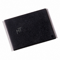
MT28F320J3RG-11 GMET TR Micron Technology Inc, MT28F320J3RG-11 GMET TR Datasheet - Page 12

MT28F320J3RG-11 GMET TR
Manufacturer Part Number
MT28F320J3RG-11 GMET TR
Description
IC FLASH 32MBIT 110NS 56TSOP
Manufacturer
Micron Technology Inc
Datasheet
1.MT28F128J3FS-12_ET_TR.pdf
(55 pages)
Specifications of MT28F320J3RG-11 GMET TR
Format - Memory
FLASH
Memory Type
FLASH
Memory Size
32M (4Mx8, 2Mx16)
Speed
110ns
Interface
Parallel
Voltage - Supply
2.7 V ~ 3.6 V
Operating Temperature
-40°C ~ 85°C
Package / Case
56-TSOP
Lead Free Status / RoHS Status
Contains lead / RoHS non-compliant
wake-up interval, normal operation is restored. The
command execution logic (CEL) is reset to the read
array mode and the status register is set to 80h.
tion, RP# LOW aborts the operation. In default mode,
STS transitions LOW and remains LOW for a maxi-
mum time of
tion is complete. Any memory content changes are no
longer valid; the data may be partially corrupted after a
program or partially changed after an erase or lock bit
configuration. After RP# goes to logic HIGH (V
after
After coming out of reset, the system expects to read
from the Flash memory. During block erase, program,
or lock bit configuration mode, automated Flash
memories provide status information when accessed.
When a CPU reset occurs with no Flash memory reset,
proper initialization may not occur because the Flash
memory may be providing status information instead
of array data. Micron Flash memories allow proper ini-
tialization following a system reset through the use of
the RP# input. RP# should be controlled by the same
RESET# signal that resets the system CPU.
Read Query
information, CFI ID string, system interface informa-
tion, device geometry information, and extended
query information. READ QUERY information is only
accessed by executing a single-word READ.
Read Identifier Codes
the manufacturer code, device code, and the block
lock configuration codes for each block (see Figure 7).
The block lock configuration codes identify locked and
unlocked blocks.
Write
device data, query, identifier codes, and reading and
clearing of the status register. In addition, when V
V
tion can also be performed.
command data and an address within the block. The
BYTE/WORD PROGRAM command requires the com-
mand and address of the location to be written to. The
09005aef80b5a323
MT28F640J3.fm – Rev. N 3/05 EN
PENH
During block erase, program, or lock bit configura-
It is important to assert RP# during system reset.
The READ QUERY operation produces block status
The READ IDENTIFIER CODES operation produces
Writing commands to the CEL allows reading of
The BLOCK ERASE command requires suitable
t
RS, another command can be written.
, block erasure, program, and lock bit configura-
t
PLPH +
t
PHRH, until the RESET opera-
IH
), and
PEN
=
12
CLEAR BLOCK LOCK BITS command requires the
command and any address within the device. Set
BLOCK LOCK BITS command requires the command
and the block to be locked. The CEL does not occupy
an addressable memory location. It is written to when
the device is enabled and WE# is LOW. The address
and data needed to execute a command are latched on
the rising edge of WE# or the first edge of CEx that dis-
ables the device (see Table 2 on page 11). Standard
microprocessor write timings are used.
NOTE:
When obtaining these identifier codes, A0 is not used in
either x8 or x16 modes. Data is always given on the
LOW byte in x16 mode (upper byte contains 00h).
Figure 7: Device Identifier Code
Micron Technology, Inc., reserves the right to change products or specifications without notice.
Memory Map
128Mb, 64Mb, 32Mb
Q-FLASH MEMORY
©2000 Micron Technology. Inc.


