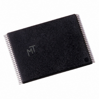
MT28F320J3RG-11 GMET TR Micron Technology Inc, MT28F320J3RG-11 GMET TR Datasheet - Page 29

MT28F320J3RG-11 GMET TR
Manufacturer Part Number
MT28F320J3RG-11 GMET TR
Description
IC FLASH 32MBIT 110NS 56TSOP
Manufacturer
Micron Technology Inc
Datasheet
1.MT28F128J3FS-12_ET_TR.pdf
(55 pages)
Specifications of MT28F320J3RG-11 GMET TR
Format - Memory
FLASH
Memory Type
FLASH
Memory Size
32M (4Mx8, 2Mx16)
Speed
110ns
Interface
Parallel
Voltage - Supply
2.7 V ~ 3.6 V
Operating Temperature
-40°C ~ 85°C
Package / Case
56-TSOP
Lead Free Status / RoHS Status
Contains lead / RoHS non-compliant
are left in an undetermined state. To initialize block
lock bit contents to known values, a repeat of CLEAR
BLOCK LOCK BITS is required.
PROTECTION REGISTER PROGRAM
Command
tion register to increase the security of a system
design. For example, the number contained in the pro-
tection register can be used for the Flash component
to communicate with other system components, such
as the CPU or ASIC, to prevent device substitution. The
128 bits of the protection register are divided into two
64-bit segments. One of the segments is programmed
at the Micron factory with a unique and unchangeable
64-bit number. The other segment is left blank for cus-
tomers to program as needed. After the customer seg-
ment is programmed, it can be locked to prevent
reprogramming.
Reading the Protection Register
read mode. The device is switched to identification
read mode by writing the READ IDENTIFIER com-
mand (90h). When in this mode, READ cycles from
addresses shown in Table 20 on page 30 or Table 21 on
page 30 retrieve the specified information. To return to
read array mode, the READ ARRAY command (FFh)
must be written.
Programming the Protection Register
two-cycle PROTECTION PROGRAM commands.
for word-wide parts and eight bits at a time for byte-
wide parts. First, the PROTECTION PROGRAM SETUP
command, C0h, is written. The next write to the device
latches in addresses and data, and programs the speci-
fied location. The allowable addresses are shown in
Table 20 on page 30 and Table 21 on page 30. Any
attempt to address PROTECTION PROGRAM com-
mands outside the defined protection register address
space results in a status register error (program error
09005aef80b5a323
MT28F640J3.fm – Rev. N 3/05 EN
The 3V Q-Flash memory includes a 128-bit protec-
The protection register is read in the identification
The protection register bits are programmed with
The 64-bit number is programmed 16 bits at a time
29
bit SR4 is set to “1”). Attempting to program a locked
protection register segment results in a status register
error (program error bit SR4 and lock error bit SR1 are
set to “1”).
Locking the Protection Register
“0,” the user-programmable segment of the protection
register is lockable. To protect the unique device num-
ber, bit 0 of this location is programmed to “0” at the
Micron factory. Bit 1 is set using the PROTECTION
PROGRAM command to program “FFFDh” to the PR-
LOCK location. When these bits have been pro-
grammed, no further changes can be made to the val-
ues stored in the protection register. PROTECTION
PROGRAM commands to a locked section will result in
a status register error (program error bit SR4 and lock
error bit SR1 are set to “1”). Note that the protection
register lockout state is not reversible.
NOTE:
Figure 8: Protection Register Memory
By programming bit 1 of the PR-LOCK location to
A0 is not used in x16 mode when accessing the protec-
tion register map (see Table 20 on page 30 for x16
addressing). A0 is used for x8 mode (see Table 21 on
page 30 for x8 addressing).
Address
Micron Technology, Inc., reserves the right to change products or specifications without notice.
Word
88h
85h
84h
81h
80h
Factory-Programmed
1 Word Lock
User-Programmed
128Mb, 64Mb, 32Mb
4 Words
4 Words
Q-FLASH MEMORY
Map
0
©2000 Micron Technology. Inc.


