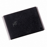
MT28F320J3RG-11 GMET TR Micron Technology Inc, MT28F320J3RG-11 GMET TR Datasheet - Page 13

MT28F320J3RG-11 GMET TR
Manufacturer Part Number
MT28F320J3RG-11 GMET TR
Description
IC FLASH 32MBIT 110NS 56TSOP
Manufacturer
Micron Technology Inc
Datasheet
1.MT28F128J3FS-12_ET_TR.pdf
(55 pages)
Specifications of MT28F320J3RG-11 GMET TR
Format - Memory
FLASH
Memory Type
FLASH
Memory Size
32M (4Mx8, 2Mx16)
Speed
110ns
Interface
Parallel
Voltage - Supply
2.7 V ~ 3.6 V
Operating Temperature
-40°C ~ 85°C
Package / Case
56-TSOP
Lead Free Status / RoHS Status
Contains lead / RoHS non-compliant
Bus Operation
conform to the standard microprocessor bus cycles.
The local CPU reads and writes Flash memory
in-system.
Table 3:
NOTE:
10. Command writes involving block erase, program, or lock bit configuration are reliably executed when V
11. Refer to
09005aef80b5a323
MT28F640J3.fm – Rev. N 3/05 EN
MODE
Read Array
Output Disable
Standby
Reset/Power-down
Mode
Read Identifier Codes
Read Query
Read Status (ISM off)
Read Status (ISM On)
DQ 7
DQ15–DQ8
DQ6–DQ0
Write
1. See
2. OE# and WE# should never be enabled simultaneously.
3. DQ refers to DQ0–DQ7 if BYTE# is LOW and DQ0–DQ15 if BYTE# is HIGH.
4. High-Z is V
5. When Vpen £ Vpenlk, memory contents can be read, but not altered. Refer to the Recommended DC Electrical Char-
6. X can be V
7. In default mode, STS is V
8. See Read Identifier Codes section for read identifier code data.
9. See Read Query Mode Command section for read query data.
All bus cycles to and from the Flash memory must
acteristics table on page 43.
V
rithms. It is V
pend mode, or reset/power-down mode.
and V
PENH
Table 2 on page 11
CC
voltages.
is within specification.
Table 4 on page 14
IL
OH
Bus Operations
or V
OH
with an external pull-up resistor.
when the ISM is not busy, in block erase suspend mode (with programming inactive), program sus-
IH
for control and address pins, and V
RP#
V
V
V
V
V
V
V
V
V
IH
IH
IH
IH
IH
IH
IH
IH
IL
OL
for valid CE configurations.
when the ISM is executing internal block erase, program, or lock bit configuration algo-
CE0, CE1,
for valid D
Disabled
Enabled
Enabled
Enabled
Enabled
Enabled
Enabled
Enabled
CE2
X
1
IN
during a WRITE operation.
OE#
V
V
V
V
V
V
V
X
X
IH
IH
IL
IL
IL
IL
IL
2
WE#
V
V
V
V
V
V
V
X
X
PENLK
IH
IH
IH
IH
IH
IH
IL
2
13
or V
See Figure 7
See Table 7
ADDRESS
PENH
X
X
X
X
X
X
X
Micron Technology, Inc., reserves the right to change products or specifications without notice.
for V
PEN
. See DC Characteristics for V
V
V
PENH
PEN
X
X
X
X
X
X
X
X
128Mb, 64Mb, 32Mb
High-Z
High-Z
High-Z
High-Z
High-Z
Q-FLASH MEMORY
D
D
DQ
D
OUT
OUT
IN
3
STS DEFAULT
High-Z
High-Z
High-Z
High-Z
MODE
X
X
X
©2000 Micron Technology. Inc.
PEN
4
4
4
4
PENLK
= V
PENH
and
5, 6, 7
7, 10, 11
NOTES
8
9


