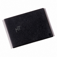
MT28F320J3RG-11 GMET TR Micron Technology Inc, MT28F320J3RG-11 GMET TR Datasheet - Page 27

MT28F320J3RG-11 GMET TR
Manufacturer Part Number
MT28F320J3RG-11 GMET TR
Description
IC FLASH 32MBIT 110NS 56TSOP
Manufacturer
Micron Technology Inc
Datasheet
1.MT28F128J3FS-12_ET_TR.pdf
(55 pages)
Specifications of MT28F320J3RG-11 GMET TR
Format - Memory
FLASH
Memory Type
FLASH
Memory Size
32M (4Mx8, 2Mx16)
Speed
110ns
Interface
Parallel
Voltage - Supply
2.7 V ~ 3.6 V
Operating Temperature
-40°C ~ 85°C
Package / Case
56-TSOP
Lead Free Status / RoHS Status
Contains lead / RoHS non-compliant
BYTE/WORD PROGRAM Commands
word program setup. This program setup (standard
40h or alternate 10h) is written, followed by a second
write that specifies the address and data (latched on
the rising edge of WE#). Next, the ISM takes over to
internally control the programming and program ver-
ify algorithms. When the program sequence is written,
the device automatically outputs status register data
when read (see Figure 10 on page 32). The CPU can
detect the completion of the program event by analyz-
ing the STS pin or status register bit SR7.
should be checked. The status register should be
cleared if a program error is detected. The ISM only
detects errors for “1s” that do not successfully program
to “0s.” The CEL remains in read status register mode
until it receives another command.
V
SR3 are set to “1” if a byte/word program is attempted
while V
should be cleared for successful byte/word programs.
If BYTE/WORD is attempted while the corresponding
block lock bit is set, SR1 and SR4 are set to “1.”
PROGRAM SUSPEND Command
gram interruption to read data in other Flash memory
locations. After starting the programming process,
writing the PROGRAM SUSPEND command requests
that the ISM suspend the program sequence at a pre-
determined point in the algorithm. When the PRO-
GRAM SUSPEND command is written, the device
continues to output status register data when read.
Polling status register bit SR7 can determine when the
programming operation has been suspended. When
SR7 = 1, SR2 is also set to “1” to indicate that the device
is in the program suspend mode. STS in RY/BY# level
mode also transitions to V
the program suspend latency.
read data from unsuspended locations. While pro-
gramming is suspended, the only other valid com-
mands are READ QUERY, READ STATUS REGISTER,
CLEAR STATUS REGISTER, CONFIGURE, and PRO-
GRAM RESUME. When the PROGRAM RESUME com-
mand is written, the ISM continues the programming
process. Status register bits SR2 and SR7 automatically
clear and STS in RY/BY# mode returns to V
PROGRAM RESUME command is written, the device
09005aef80b5a323
MT28F640J3.fm – Rev. N 3/05 EN
CC
A two-cycle command sequence executes a byte/
Upon program completion, status register bit SR4
Reliable byte/word programs can only occur when
The PROGRAM SUSPEND command enables pro-
Hence, a READ ARRAY command can be written to
and V
PEN
PEN
≤ V
PENLK
are valid. Status register bits SR4 and
. The corresponding block lock bit
OH
. Note that
t
OL
LPS defines
. After the
27
automatically outputs status register data when read.
V
valid V
programming) while in program suspend mode. Refer
to Figure 11 on page 33 (PROGRAM SUSPEND/
RESUME Flowchart).
SET READ CONFIGURATION Command
CONFIGURATION command. The devices default to
the asynchronous page mode. If this command is
given, the operation of the device will not be affected.
READ Configuration
nous page mode and standard word/byte READs with-
out configuration requirement. Status register and
identifier only support standard word/byte single
READ operations.
STS CONFIGURATION Command
pin can be configured to different states. Once config-
ured, the STS pin remains in that configuration until
another configuration command is issued, RP# is
asserted low, or the device is powered down. Initially,
the STS pin defaults to RY/BY# operation where RY/
BY# goes LOW to indicate that the state machine is
busy. When HIGH, RY/BY# indicates that either the
state machine is ready for a new operation or it is sus-
pended. Table 19 on page 28, Configuration Coding
Definitions, shows the possible STS configurations. To
change the STS pin to other modes, the CONFIGURA-
TION command is given, followed by the desired con-
figuration code. The three alternate configurations are
all pulse modes and may be used as a system interrupt.
With these configurations, bit 0 controls erase com-
plete interrupt pulse, and bit 1 controls program com-
plete interrupt pulse. Providing the 00h configuration
code with the CONFIGURATION command resets the
STS pin to the default RY/BY# level mode. Table 19 on
page 28 describes possible configurations and usage.
The CONFIGURATION command can only be given
when the device is not busy or suspended. When con-
figured in one of the pulse modes, the STS pin pulses
LOW with a typical pulse width of 250ns. Check SR7 for
device status. An invalid configuration code results in
status register bits SR4 and SR5 being set to “1.”
PEN
Q-Flash memory does not support the SET READ
Micron’s Q-Flash devices support both asynchro-
Using the CONFIGURATION command, the STS
Micron Technology, Inc., reserves the right to change products or specifications without notice.
must remain at V
CC
levels (the same V
128Mb, 64Mb, 32Mb
Q-FLASH MEMORY
PENH
PEN
and V
and V
CC
CC
©2000 Micron Technology. Inc.
must remain at
levels used for


