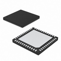
MAX17017GTM+ Maxim Integrated Products, MAX17017GTM+ Datasheet - Page 16

MAX17017GTM+
Manufacturer Part Number
MAX17017GTM+
Description
IC PWR SUPPLY CONTROLLER 48TQFN
Manufacturer
Maxim Integrated Products
Datasheet
1.MAX17017GTM.pdf
(31 pages)
Specifications of MAX17017GTM+
Applications
Power Supply Controller
Voltage - Input
5.5 ~ 28 V
Operating Temperature
-40°C ~ 105°C
Mounting Type
Surface Mount
Package / Case
48-TQFN Exposed Pad
Input Voltage
5.5 V to 24 V
Operating Temperature Range
- 40 C to + 105 C
Mounting Style
SMD/SMT
Duty Cycle (max)
300 uA
Supply Voltage Range
3V To 5V, 5.5V To 28V
Digital Ic Case Style
TQFN
No. Of Pins
48
Termination Type
SMD
No. Of Channels
4
Rohs Compliant
Yes
Filter Terminals
SMD
Leaded Process Compatible
Yes
Lead Free Status / RoHS Status
Lead free / RoHS Compliant
Current - Supply
-
Voltage - Supply
-
Lead Free Status / Rohs Status
Lead free / RoHS Compliant
Quad-Output Controller for
Low-Power Architecture
The MAX17017 standard application circuit (Figure 1)
provides a 5V/5A
and 0.9A/2A VTT outputs for DDR, and a 1.05V/5A
chipset supply.
The MAX17017 supports four power outputs—one high-
voltage step-down controller, two internal MOSFET
step-down switching regulators, and one high-current
source/sink linear regulator. The step-down switching
regulators use a current-mode fixed-frequency architec-
ture compensated by the output capacitance. An inter-
nal 50mA 5V linear regulator provides the bias supply
and driver supplies, allowing the controller to power up
from input supplies greater than 5.5V.
An internal linear regulator produces a preset 5V low-
current output from INLDO. LDO5 powers the gate dri-
vers for the external MOSFETs, and provides the bias
16
40–43
PIN
36
37
38
39
44
45
46
47
48
EP
______________________________________________________________________________________
Fixed 5V Linear Regulator (LDO5)
NAME
POKD
PGND
SYNC
INBC
ONB
ONA
OND
ONC
FBB
V
FBC
DD
P-P
Feedback Input for the Internal 3A Step-Down Converter. FBB regulates to 0.75V.
Switching Regulator B Enable Input. When ONB is pulled low, LXB is high impedance. When ONB is driven
high, the controller enables the 3A internal switching regulator.
External Synchronization Input. Used to override the internal switching frequency.
Switching Regulator A Enable Input. When ONA is pulled low, DLA and DHA are pulled low. When ONA is
driven high, the controller enables the step-up/step-down converter.
Input for Regulators B and C. Power INBC from a 2.5V to 5.5V supply. Internally connected to the drain of
the high-side MOSFETs for both regulator B and regulator C. Bypass to PGND with 2x 10μF or greater
ceramic capacitors to support the RMS current.
5V Bias Supply Input for the Internal Switching Regulator Drivers. Bypass with a 1μF or greater ceramic
capacitor. Provides power for the BSTB and BSTC driver supplies.
Open-Drain Power-Good Output for the Internal Source/Sink Linear Regulator. POKD is low if FBD is more
than 10% (typ) above or below the REFIND regulation threshold. POKD is held low during soft-start and in
shutdown. POKD becomes high impedance when FBD is in regulation.
S our ce/S i nk Li near Reg ul ator ( Reg ul ator D ) and Refer ence Buffer E nab l e Inp ut. W hen O N D i s p ul l ed l ow , O U TD
i s hi g h i m p ed ance. W hen O N D i s d r i ven hi g h, the contr ol l er enab l es the sour ce/si nk l i near r eg ul ator .
Switching Regulator C Enable Input. When ONC is pulled low, LXC is high impedance. When ONC is driven
high, the controller enables the 5A internal switching regulator.
Feedback Input for the Internal 5A Step-Down Converter. FBC regulates to 0.75V.
Power Ground. The source of the low-side MOSFETs (REG B and REG C), the drivers for all switching
regulators, and the sink MOSFET of the VTT LDO are all internally connected to the exposed pad.
Connect the exposed backside pad to system power ground planes through multiple vias.
main stage, a 1.8V/3A
Detailed Description
P-P
VDDQ
P-P
supply required for the SMPS analog controller, refer-
ence, and logic blocks. LDO5 supplies at least 50mA
for external and internal loads, including the MOSFET
gate drive, which typically varies from 5mA to 15mA
per switching regulator, depending on the switching
frequency. Bypass LDO5 with a 4.7μF or greater
ceramic capacitor to guarantee stability under the full-
load conditions.
The MAX17017 switch-mode step-down switching reg-
ulators require a 5V bias supply in addition to the main-
power input supply. This 5V bias supply is generated
by the controller’s internal 5V linear regulator (LDO5).
This boot-strappable LDO allows the controller to
power up independently. The gate-driver V
supply is typically connected to the fixed 5V linear reg-
ulator output (LDO5). Therefore, the 5V LDO supply
must provide LDO5 (PWM controller) and the gate-
drive power during power-up.
FUNCTION
Pin Description (continued)
DD
input


