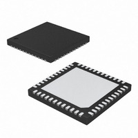
MAX17017GTM+ Maxim Integrated Products, MAX17017GTM+ Datasheet - Page 21

MAX17017GTM+
Manufacturer Part Number
MAX17017GTM+
Description
IC PWR SUPPLY CONTROLLER 48TQFN
Manufacturer
Maxim Integrated Products
Datasheet
1.MAX17017GTM.pdf
(31 pages)
Specifications of MAX17017GTM+
Applications
Power Supply Controller
Voltage - Input
5.5 ~ 28 V
Operating Temperature
-40°C ~ 105°C
Mounting Type
Surface Mount
Package / Case
48-TQFN Exposed Pad
Input Voltage
5.5 V to 24 V
Operating Temperature Range
- 40 C to + 105 C
Mounting Style
SMD/SMT
Duty Cycle (max)
300 uA
Supply Voltage Range
3V To 5V, 5.5V To 28V
Digital Ic Case Style
TQFN
No. Of Pins
48
Termination Type
SMD
No. Of Channels
4
Rohs Compliant
Yes
Filter Terminals
SMD
Leaded Process Compatible
Yes
Lead Free Status / RoHS Status
Lead free / RoHS Compliant
Current - Supply
-
Voltage - Supply
-
Lead Free Status / Rohs Status
Lead free / RoHS Compliant
Power-on reset (POR) occurs when V
approximately 1.9V, resetting the undervoltage, overvolt-
age, and thermal-shutdown fault latches. The POR cir-
cuit also ensures that the low-side drivers are pulled low
until the SMPS controllers are activated. The V
undervoltage lockout (UVLO) circuitry prevents the
switching regulators from operating if the 5V bias supply
(V
Once the 5V bias supply rises above this input UVLO
threshold and ONA is pulled high, the main step-down
controller (regulator A) is enabled and begins switch-
ing. The internal voltage soft-start gradually increments
the feedback voltage by 10mV every 12 switching
cycles. Therefore, OUTA reaches its nominal regulation
voltage 1200/f
REG A Startup Waveform (Heavy Load) graph in the
Typical Operating Characteristics ).
The internal step-down controllers start switching and the
output voltages ramp up using soft-start. If the bias sup-
ply voltage drops below the UVLO threshold, the controller
stops switching and disables the drivers (LX_ becomes
high impedance) until the bias supply voltage recovers.
Once the 5V bias supply and INBC rise above their
respective input UVLO thresholds (SHDN must be
pulled high to enable the reference), and ONB or ONC
is pulled high, the respective internal step-down con-
troller (regulator B or C) becomes enabled and begins
switching. The internal voltage soft-start gradually
increments the feedback voltage by 10mV every 24
switching cycles for regulator B or every 12 switching
cycles for regulator C. Therefore, OUTB reaches its
nominal regulation voltage 1800/f
is enabled, and OUTC reaches its nominal regulation
voltage 900/f
REG B Startup Waveform (Heavy Load) and REG C
Startup Waveform (Heavy Load) graphs in the Typical
Operating Characteristics ).
POKA, POKB, and POKC are the open-drain outputs of
window comparators that continuously monitor each
output for undervoltage and overvoltage conditions.
POK_ is actively held low in shutdown (SHDN = GND),
standby (ONA = ONB = ONC = GND), and soft-start.
Once the soft-start sequence terminates, POK_
CC
and V
DD
SMPS Power-Good Outputs (POK)
SWC
SMPS POR, UVLO, and Soft-Start
) is below its 4.2V UVLO threshold.
SWA
______________________________________________________________________________________
after regulator C is enabled (see the
after regulator A is enabled (see the
Regulator B and C Startup
SWB
Regulator A Startup
after regulator B
CC
rises above
CC
input
Quad-Output Controller for
Low-Power Architecture
becomes high impedance as long as the output remains
within ±8% (min) of the nominal regulation voltage set
by FB_. POK_ goes low once its corresponding output
drops 12% (typ) below its nominal regulation point, an
output overvoltage fault occurs, or the output is shut
down. For a logic-level POK_ output voltage, connect an
external pullup resistor between POK_ and LDO5. A
100kΩ pullup resistor works well in most applications.
If the output voltage rises above 112% (typ) of its nomi-
nal regulation voltage, the controller sets the fault latch,
pulls POK_ low, shuts down the respective regulator,
and immediately pulls the output to ground through its
low-side MOSFET. Turning on the low-side MOSFET
with 100% duty cycle rapidly discharges the output
capacitors and clamps the output to ground. However,
this commonly undamped response causes negative
output voltages due to the energy stored in the output
LC at the instant the OVP occurs. If the load cannot tol-
erate a negative voltage, place a power Schottky diode
across the output to act as a reverse-polarity clamp. If
the condition that caused the overvoltage persists
(such as a shorted high-side MOSFET), the input
source also fails (short-circuit fault). Cycle V
1V or toggle the respective enable input to clear the
fault latch and restart the regulator.
Each MAX17017 includes an output undervoltage
(UVP)-protection circuit that begins to monitor the out-
put once the startup blanking period has ended. If any
output voltage drops below 88% (typ) of its nominal
regulation voltage, the UVP protection immediately sets
the fault latch, pulls the respective POK output low,
forces the high-side and low-side MOSFETs into high-
impedance states (DH = DL = low), and shuts down the
respective regulator. Cycle V
respective enable input to clear the fault latch and
restart the regulator.
The MAX17017 features a thermal-fault-protection cir-
cuit. When the junction temperature rises above
+160°C, a thermal sensor activates the fault latch, pulls
all POK outputs low, and shuts down all regulators.
Toggle SHDN to clear the fault latch and restart the
controllers after the junction temperature cools by 15°C.
Output Undervoltage Protection (UVP)
Output Overvoltage Protection (OVP)
SMPS Fault Protection
Thermal-Fault Protection
CC
below 1V or toggle the
CC
below
21


