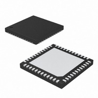
MAX17017GTM+ Maxim Integrated Products, MAX17017GTM+ Datasheet - Page 23

MAX17017GTM+
Manufacturer Part Number
MAX17017GTM+
Description
IC PWR SUPPLY CONTROLLER 48TQFN
Manufacturer
Maxim Integrated Products
Datasheet
1.MAX17017GTM.pdf
(31 pages)
Specifications of MAX17017GTM+
Applications
Power Supply Controller
Voltage - Input
5.5 ~ 28 V
Operating Temperature
-40°C ~ 105°C
Mounting Type
Surface Mount
Package / Case
48-TQFN Exposed Pad
Input Voltage
5.5 V to 24 V
Operating Temperature Range
- 40 C to + 105 C
Mounting Style
SMD/SMT
Duty Cycle (max)
300 uA
Supply Voltage Range
3V To 5V, 5.5V To 28V
Digital Ic Case Style
TQFN
No. Of Pins
48
Termination Type
SMD
No. Of Channels
4
Rohs Compliant
Yes
Filter Terminals
SMD
Leaded Process Compatible
Yes
Lead Free Status / RoHS Status
Lead free / RoHS Compliant
Current - Supply
-
Voltage - Supply
-
Lead Free Status / Rohs Status
Lead free / RoHS Compliant
the selected inductance value, the actual peak-to-peak
inductor ripple current (ΔI
Ferrite cores are often the best choice, although soft sat-
urating molded core inductors are inexpensive and can
work well at 500kHz. The core must be large enough not
to saturate at the peak inductor current (I
The output filter capacitor selection requires careful
evaluation of several different design requirements—
stability, transient response, and output ripple volt-
age—that place limits on the output capacitance and
ESR. Based on these requirements, the typical applica-
tion requires a low-ESR polymer capacitor (lower cost
but higher output-ripple voltage) or bulk ceramic
capacitors (higher cost but low output-ripple voltage).
Voltage positioning dynamically lowers the output volt-
age in response to the load current, reducing the loop
gain. This reduces the output capacitance requirement
(stability and transient) and output power dissipation
requirements as well. The load-line is generated by sens-
ing the inductor current through the high-side MOSFET
on-resistance, and is internally preset to -5mV/A (typ) for
regulator B and -7mV/A (typ) for regulator C. The load-
line ensures that the output voltage remains within the
regulation window over the full-load conditions.
The load line of the internal SMPS regulators also pro-
vides the AC ripple voltage required for stability. To
maintain stability, the output capacitive ripple must be
kept smaller than the internal AC ripple voltage, and
crossover must occur before the Nyquist pole—
(2f
a minimum output capacitance can be determined from
the following:
When using only ceramic capacitors on the output, the
required output capacitance is:
where R
regulator B, or 7mV/A for regulator C as defined in the
SW
)/(1+D) occurs. Based on these loop requirements,
C
OUT
DROOP
I
PEAK
>
ΔI
SMPS Output Capacitor Selection
⎛
⎜
⎝
INDUCTOR
2
f
=
SW DROOP
is 2R
I
LOAD MAX
______________________________________________________________________________________
R
1
SENSE
(
=
INDUCTOR
V
SMPS Loop Compensation
OUT
)
⎞
⎟
⎠
for regulator A, 5mV/A for
+
⎛
⎜
⎝
V f
⎛
⎜
⎝
V
(
IN SW
V
OUT
V
Δ
FB
IN
I
INDUCTOR
) is defined by:
−
⎞
⎟
⎠
L
V
2
⎛
⎜
⎝
OUT
1
PEAK
+
)
V
OUT
V
⎞
⎟
⎠
):
IN
⎞
⎟
⎠
Quad-Output Controller for
Low-Power Architecture
Electrical Characteristics table, and f
frequency selected by the FREQ setting (see Table 1).
When using only polymer capacitors on the output, the
additional ESR of the output (R
consideration.
For duty cycles less than 40% using polymer capacitors:
For duty cycles above 40% using polymer capacitors, the
ESR and C
When the ESR condition described above is not satis-
fied, or when using a mix of ceramic and polymer
capacitors on the output, an additional feedback pole-
capacitor from FB to analog ground (C
to cancel the output capacitor ESR zero:
where R
divider.
With polymer capacitors, the effective series resistance
(ESR) dominates and determines the output ripple volt-
age. The step-down regulator’s output ripple voltage
(V
(ΔI
Therefore, the maximum ESR to meet the output ripple
voltage requirement is:
where f
citance value required relates to the physical case size
needed to achieve the ESR requirement, as well as to
the capacitor chemistry. Thus, polymer capacitor selec-
tion is usually limited by ESR and voltage rating rather
than by capacitance value. Alternatively, combining
ceramics (for the low ESR) and polymers (for the bulk
capacitance) helps balance the output capacitance vs.
output ripple voltage requirements.
C
RIPPLE
OUT
INDUCTOR
>
R
C
⎛
⎜
⎝
SW
ESR
OUT
2
FB
f
SW
) equals the total inductor ripple current
R
OUT
is the switching frequency. The actual capa-
is the parallel impedance of the FB resistive
ESR
(
>
R
<
) multiplied by the output capacitor’s ESR.
C
DROOP
⎛
⎜
⎝
must meet the conditions listed below:
FB
R
2
≤
f
DROOP
SW DROOP
⎡
⎢
⎢
⎣
>
(
V
R
+
IN
⎛
⎜
⎝
1
R
C OUT R
1
ESR
V f
−
IN SW
⎛
⎜
⎝
V
SMPS Output Ripple Voltage
R FB
V
OUT
V
x V
OUT
FB
⎞
⎟
⎠
L
FB
ESR
⎛
⎜
⎝
)
V
⎞
⎟
⎠
ESR
V
OUT
/
V
OUT
FB
V
⎞
⎟
⎠
OUT
) must be taken into
SW
⎤
⎥
⎥
⎦
⎞
⎟
⎠
)
V
⎛
⎜
⎝
⎞
⎟
⎠
RIPPLE
1
⎛
⎜
⎝
FB
is the switching
V
V
+
OUT
) is necessary
FB
V
⎞
⎟
⎠
OUT
V
⎛
⎜
⎝
IN
1
+
⎞
⎟
⎠
V
OUT
V
IN
23
⎞
⎟
⎠


