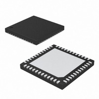
MAX17017GTM+ Maxim Integrated Products, MAX17017GTM+ Datasheet - Page 27

MAX17017GTM+
Manufacturer Part Number
MAX17017GTM+
Description
IC PWR SUPPLY CONTROLLER 48TQFN
Manufacturer
Maxim Integrated Products
Datasheet
1.MAX17017GTM.pdf
(31 pages)
Specifications of MAX17017GTM+
Applications
Power Supply Controller
Voltage - Input
5.5 ~ 28 V
Operating Temperature
-40°C ~ 105°C
Mounting Type
Surface Mount
Package / Case
48-TQFN Exposed Pad
Input Voltage
5.5 V to 24 V
Operating Temperature Range
- 40 C to + 105 C
Mounting Style
SMD/SMT
Duty Cycle (max)
300 uA
Supply Voltage Range
3V To 5V, 5.5V To 28V
Digital Ic Case Style
TQFN
No. Of Pins
48
Termination Type
SMD
No. Of Channels
4
Rohs Compliant
Yes
Filter Terminals
SMD
Leaded Process Compatible
Yes
Lead Free Status / RoHS Status
Lead free / RoHS Compliant
Current - Supply
-
Voltage - Supply
-
Lead Free Status / Rohs Status
Lead free / RoHS Compliant
The switching frequency and inductor operating point
determine the inductor value as follows:
Choose an available inductor value from an appropriate
inductor family. Calculate the maximum DC input cur-
rent at the minimum input voltage V
servation of energy:
Calculate the ripple current at that operating point and
the peak current required for the inductor:
The inductor’s saturation current rating and the
MAX17017’s LXA current limit should exceed I
the inductor’s DC current rating should exceed
I
with less than 0.1Ω series resistance.
For boost converter, during continuous operation, the
output capacitor has a trapezoidal current profile. The
large RMS ripple current in the output capacitor must
be rated to handle the current. The RMS current is
greatest at I
age. Therefore, the output capacitor should be chosen
with a rating at least I
the capacitor is then given by:
The total output voltage ripple has two components: the
capacitive ripple caused by the charging and discharg-
ing of the output capacitance, and the resistive ripple
due to the capacitor’s equivalent series resistance (ESR):
VIN(DC,MAX)
Step-Up Configuration Inductor Selection
I
PEAK
L
I
LOAD(MAX)
COUT RMS
I
VIN DC MAX
ΔI
. For good efficiency, choose an inductor
=
INDUCTOR
⎛
⎜
⎝
(
=
V
(
Step-Up Configuration Output
V
OUT
I
LOAD MAX
______________________________________________________________________________________
IN
,
)
⎞
⎟
⎠
COUT(RMS).
2
)
≅
and minimum input working volt-
(
=
⎛
⎜ ⎜
⎝
=
I
LOAD
I
LOAD MAX SW
I
LOAD MAX OUT
V
IN
)
V
+
V
(
Capacitor Selection
OUT
OUT SW
V
⎛
⎜
⎝
V
(
IN MIN
(
Δ
OUT
V
I
INDUCTOR
OUT
(
The RMS current into
f
-
V
V
)
)
f
-
2
IN
VIN
IN(MIN)
V
)
V
L
-
IN
V
LIR
IN
)
⎞
⎟
⎠
⎞
⎟
⎠
using con-
PEAK
Quad-Output Controller for
and
Low-Power Architecture
and:
where I
capacitors, the output voltage ripple is typically domi-
nated by resistive ripple voltage. The voltage rating and
temperature characteristics of the output capacitor
must also be considered. The output ripple voltage due
to the frequency-dependent term can be compensated
by using capacitors of very low ESR to maintain low rip-
ple voltage. Note that all ceramic capacitors typically
have large temperature coefficient and bias voltage
coefficients. The actual capacitor value in circuit is typi-
cally significantly less than the stated value.
The boost converter small-signal model contains a right
half-plane (RHP) zero. The presence of an RHP zero
tends to destabilize wide-bandwidth feedback loop
because during a transient, the output initially changes
in the wrong direction. Also when an RHP zero is pre-
sent, it is difficult to obtain an adequate phase margin.
RHP is determined by inductance L, duty cycle D
and load R. The RHP is:
To maintain stability, crossover must occur before the
RHP. To make sure the phase margin is big enough to
stabilize the circuit, the converter crossover must be
kept 4 ~ 10 times slower than the RHP zero. A minimum
output capacitance is determined from the following:
where A
er gain divided by the current-sense gain; R
rent-sensing resistor.
Additionally, an additional feedback pole—capacitor
from FB to analog ground (C
cancel the unwanted ESR zero of the output capacitor.
PEAK
C
STEP-UP
Step-Up Configuration Loop Compensation
OUT
V
V
RIPPLE
RIPPLE C
is the peak inductor current. For polymer
>
V
4
is equal to 1.25, which is the error amplifi-
RIPPLE ESR
⎛
⎜
⎝
=
f
( )
A
RHP
STEP UP
V
R
RIPPLE C
≈
(
CS
=
C
I
-
OUT
(
OUT
1
)
-
( )
≈
⎞
⎟
⎠
FB
D
2
I
⎛
⎜
⎝
PEAK ESR
⎛
⎜
⎝
UP
π
)—might be necessary to
+
V
V
L
OUT
V
V
OUT
)
OUT SW
RIPPLE ESR
2
R
R
V
(
1
REF
-
f
-
V
IN
(
D
UP
⎞
⎟
⎠
CS
)
)
R
is the cur-
L
⎞ ⎞
⎟
⎠
up
27
,


