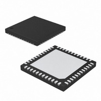
MAX17017GTM+ Maxim Integrated Products, MAX17017GTM+ Datasheet - Page 25

MAX17017GTM+
Manufacturer Part Number
MAX17017GTM+
Description
IC PWR SUPPLY CONTROLLER 48TQFN
Manufacturer
Maxim Integrated Products
Datasheet
1.MAX17017GTM.pdf
(31 pages)
Specifications of MAX17017GTM+
Applications
Power Supply Controller
Voltage - Input
5.5 ~ 28 V
Operating Temperature
-40°C ~ 105°C
Mounting Type
Surface Mount
Package / Case
48-TQFN Exposed Pad
Input Voltage
5.5 V to 24 V
Operating Temperature Range
- 40 C to + 105 C
Mounting Style
SMD/SMT
Duty Cycle (max)
300 uA
Supply Voltage Range
3V To 5V, 5.5V To 28V
Digital Ic Case Style
TQFN
No. Of Pins
48
Termination Type
SMD
No. Of Channels
4
Rohs Compliant
Yes
Filter Terminals
SMD
Leaded Process Compatible
Yes
Lead Free Status / RoHS Status
Lead free / RoHS Compliant
Current - Supply
-
Voltage - Supply
-
Lead Free Status / Rohs Status
Lead free / RoHS Compliant
and is reasonably priced. Ensure that the MAX17017
DLA gate driver can supply sufficient current to support
the gate charge and the current injected into the para-
sitic drain-to-gate capacitor caused by the high-side
MOSFET turning on; otherwise, cross-conduction prob-
lems might occur. Switching losses are not an issue for
the low-side MOSFET since it is a zero-voltage
switched device when used in the step-down topology.
Worst-case conduction losses occur at the duty factor
extremes. For the high-side MOSFET (N
case power dissipation due to resistance occurs at
minimum input voltage:
Generally, use a small high-side MOSFET to reduce
switching losses at high input voltages. However, the
R
pation limits often limits how small the MOSFET can be.
The optimum occurs when the switching losses equal
the conduction (R
losses do not become an issue until the input is greater
than approximately 15V.
Calculating the power dissipation in high-side
MOSFETs (N
it must allow for difficult-to-quantify factors that influence
the turn-on and turn-off times. These factors include the
internal gate resistance, gate charge, threshold voltage,
source inductance, and PC board (PCB) layout charac-
teristics. The following switching loss calculation pro-
vides only a very rough estimate and is no substitute for
breadboard evaluation, preferably including verification
using a thermocouple mounted on N
where C
the charge needed to turn on the N
I
Switching losses in the high-side MOSFET can become
a heat problem when maximum AC adapter voltages
are applied, due to the squared term in the switching-
loss equation (C x V
chosen for adequate R
becomes extraordinarily hot when subjected to
V
lower parasitic capacitance.
GATE
DS(ON)
IN(MAX)
PD N
is the peak gate-drive source/sink current (1A typ).
⎛
⎜
⎝
I
LOAD G SW
OSS
(
required to stay within package power-dissi-
, consider choosing another MOSFET with
H
I
GATE
H
is the output capacitance of N
Re
Q
) due to switching losses is difficult, since
sistive
(
______________________________________________________________________________________
DS(ON)
PD N Switching
)
IN
+
(
2 x f
)
C
=
DS(ON)
H
OSS IN M
⎛
⎜
⎝
) losses. High-side switching
Power-MOSFET Dissipation
SW
V
OUT
V
V
IN
2
). If the high-side MOSFET
(
at low battery voltages
⎞
⎟
⎠
(
A A X
I
LOAD
)
)
=
H
⎞
⎟
⎠
:
V
H
IN MAX SW
)
2
MOSFET, and
(
H
R
), the worst-
DS ON
H
, Q
(
)
f
G(SW)
)
Quad-Output Controller for
is
Low-Power Architecture
For the low-side MOSFET (N
dissipation always occurs at maximum battery voltage:
The absolute worst case for MOSFET power dissipation
occurs under heavy overload conditions that are
greater than I
exceed the current limit and cause the fault latch to trip.
To protect against this possibility, “overdesign” the cir-
cuit to tolerate:
where I
limit circuit, including threshold tolerance and sense-
resistance variation. The MOSFETs must have a relatively
large heatsink to handle the overload power dissipation.
Choose a Schottky diode (D
drop low enough to prevent the low-side MOSFET’s
body diode from turning on during the dead time. As a
general rule, select a diode with a DC current rating
equal to 1/3 the load current. This diode is optional and
can be removed if efficiency is not critical.
Regulator A can be configured as a step-up converter
(Figure 4). When UP/DN is pulled low, regulator A oper-
ates as a step-up converter (for 1 Li+ cell applications). It
typically generates a 5V output voltage from a 3V to 5V
battery input voltage. The step-up converter uses a cur-
rent-mode architecture; the difference between the feed-
back voltage and a 1V reference signal generates an error
signal that programs the peak inductor current to regulate
the output voltage. The step-up converter is internally com-
pensated, reducing external component requirements.
When regulator A is configured as a step-up converter,
SHDN should be connected to GND. ONA is the master
enable switch. ONA rising enables REF and the bias
block. Connect LDO5 and INLDO together with OUTA
and connect BYP to either OUTA or INA.
At light loads, efficiency is enhanced by an idle mode
in which switching occurs only as needed to service the
load. This idle-mode threshold is determined by com-
paring the current-sense signal to an internal reference.
In idle mode, the synchronous rectifier shuts off once
the current-sense voltage (CSPA - CSNA) drops below
1mV, preventing negative inductor current.
PD N
(
L
LIMIT
Re
I
sistive
LOAD
is the peak current allowed by the current-
LOAD(MAX)
Converter Configuration
)
=
=
I
LIMIT
⎡
⎢
⎢
⎣
1
Regulator A Step-Up
−
⎛
⎜
⎝
, but are not high enough to
V
−
IN MAX
⎛
⎜
⎝
V
OUT
(
Δ
L
L
I
INDUCTOR
) with a forward voltage
) the worst-case power
)
2
⎞
⎟
⎠
⎤
⎥
⎥
⎦
(
I
LOAD
⎞
⎟
⎠
)
2
R
DS ON
(
)
25


