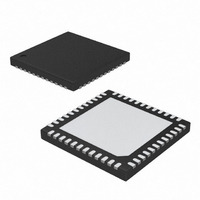
MAX17017GTM+ Maxim Integrated Products, MAX17017GTM+ Datasheet - Page 29

MAX17017GTM+
Manufacturer Part Number
MAX17017GTM+
Description
IC PWR SUPPLY CONTROLLER 48TQFN
Manufacturer
Maxim Integrated Products
Datasheet
1.MAX17017GTM.pdf
(31 pages)
Specifications of MAX17017GTM+
Applications
Power Supply Controller
Voltage - Input
5.5 ~ 28 V
Operating Temperature
-40°C ~ 105°C
Mounting Type
Surface Mount
Package / Case
48-TQFN Exposed Pad
Input Voltage
5.5 V to 24 V
Operating Temperature Range
- 40 C to + 105 C
Mounting Style
SMD/SMT
Duty Cycle (max)
300 uA
Supply Voltage Range
3V To 5V, 5.5V To 28V
Digital Ic Case Style
TQFN
No. Of Pins
48
Termination Type
SMD
No. Of Channels
4
Rohs Compliant
Yes
Filter Terminals
SMD
Leaded Process Compatible
Yes
Lead Free Status / RoHS Status
Lead free / RoHS Compliant
Current - Supply
-
Voltage - Supply
-
Lead Free Status / Rohs Status
Lead free / RoHS Compliant
Power loss in the MAX17017 VTT LDO is significant and
can become a limiting design factor in the overall
MAX17017 design:
The 1.8W total power dissipation is within the 40-pin
TQFN multilayer board power-dissipation specification
of 2.9W. The typical DDR termination application does
not actually continuously source or sink high currents.
The actual VTT current typically remains around 100mA
to 200mA under steady-state conditions. VTTR is down
in the microampere range, though the Intel specifica-
tion requires 3mA for DDR1 and 1mA for DDR2. True
worst-case power dissipation occurs on an output
short-circuit condition with worst-case current limit.
MAX17017 does not employ any foldback current limit-
ing, and relies on the internal thermal shutdown for pro-
tection. Both the VTT and VTTR output voltages are
referenced to the same REFIND input.
The minimum input operating voltage (dropout voltage) is
restricted by the maximum duty-cycle specification (see
the Electrical Characteristics table). For the best dropout
performance, use the slowest switching frequency setting
(FREQ = GND). However, keep in mind that the transient
performance gets worse as the step-down regulators
approach the dropout voltage, so bulk output capaci-
tance must be added (see the voltage sag and soar
equations in the Design Procedure section). The absolute
point of dropout occurs when the inductor current ramps
down during the off-time (ΔI
up during the on-time (ΔI
operating voltage defined by the following equation:
where V
the charge and discharge paths, respectively. A rea-
sonable minimum value for h is 1.5, while the absolute
minimum input voltage is calculated with h = 1.
The MAX17017 controller includes a minimum on-time
specification, which determines the maximum input
operating voltage that maintains the selected switching
frequency (see the Electrical Characteristics table).
Operation above this maximum input voltage results in
pulse skipping to avoid overcharging the output. At the
beginning of each cycle, if the output voltage is still
V
IN MIN
(
CHG
)
=
V
and V
OUT
PD
Applications Information
VTT
______________________________________________________________________________________
+
DIS
VTT LDO Power Dissipation
V
CHG
= 2A x 0.9V = 1.8W
are the parasitic voltage drops in
UP
+
DOWN
). This results in a minimum
h
⎛
⎜
⎝
D
Maximum Input Voltage
Minimum Input Voltage
MAX
1
) as much as it ramps
−
1
⎞
⎟
⎠
(
V
OUT
+
V
DIS
Quad-Output Controller for
)
Low-Power Architecture
above the feedback threshold voltage, the controller
does not trigger an on-time pulse, effectively skipping a
cycle. This allows the controller to maintain regulation
above the maximum input voltage, but forces the con-
troller to effectively operate with a lower switching fre-
quency. This results in an input threshold voltage at
which the controller begins to skip pulses (V
where f
FREQ.
Careful PCB layout is critical to achieving low switching
losses and clean, stable operation. The switching power
stage requires particular attention. If possible, mount all
the power components on the top side of the board,
with their ground terminals flush against one another.
Follow the MAX17017 Evaluation Kit layout and use the
following guidelines for good PCB layout:
• Keep the high-current paths short, especially at the
• Keep the power traces and load connections short.
• Minimize current-sensing errors by connecting
• When trade-offs in trace lengths must be made, it is
• Route high-speed switching nodes (BST_, LX_,
ground terminals. This practice is essential for sta-
ble, jitter-free operation.
This practice is essential for high efficiency. Using
thick copper PCBs (2oz vs. 1oz) can enhance full-
load efficiency by 1% or more. Correctly routing PCB
traces is a difficult task that must be approached in
terms of fractions of centimeters, where a single mil-
liohm of excess trace resistance causes a measur-
able efficiency penalty.
CSPA and CSNA directly across the current-sense
resistor (R
preferable to allow the inductor charging path to be
made longer than the discharge path. For example,
it is better to allow some extra distance between the
input capacitors and the high-side MOSFET than to
allow distance between the inductor and the low-
side MOSFET or between the inductor and the out-
put filter capacitor.
DHA, and DLA) away from sensitive analog areas
(REF, REFIND, FB_, CSPA, CSNA).
OSC
V
IN SKIP
SENSE_
is the switching frequency selected by
(
)
).
=
V
OUT
PCB Layout Guidelines
⎛
⎜
⎝
f
OSC ON MIN
t
1
(
)
⎞
⎟
⎠
IN(SKIP)
):
29


