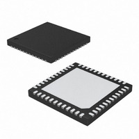
MAX17017GTM+ Maxim Integrated Products, MAX17017GTM+ Datasheet - Page 2

MAX17017GTM+
Manufacturer Part Number
MAX17017GTM+
Description
IC PWR SUPPLY CONTROLLER 48TQFN
Manufacturer
Maxim Integrated Products
Datasheet
1.MAX17017GTM.pdf
(31 pages)
Specifications of MAX17017GTM+
Applications
Power Supply Controller
Voltage - Input
5.5 ~ 28 V
Operating Temperature
-40°C ~ 105°C
Mounting Type
Surface Mount
Package / Case
48-TQFN Exposed Pad
Input Voltage
5.5 V to 24 V
Operating Temperature Range
- 40 C to + 105 C
Mounting Style
SMD/SMT
Duty Cycle (max)
300 uA
Supply Voltage Range
3V To 5V, 5.5V To 28V
Digital Ic Case Style
TQFN
No. Of Pins
48
Termination Type
SMD
No. Of Channels
4
Rohs Compliant
Yes
Filter Terminals
SMD
Leaded Process Compatible
Yes
Lead Free Status / RoHS Status
Lead free / RoHS Compliant
Current - Supply
-
Voltage - Supply
-
Lead Free Status / Rohs Status
Lead free / RoHS Compliant
Quad-Output Controller for
Low-Power Architecture
ABSOLUTE MAXIMUM RATINGS
INLDO, SHDN to GND............................................-0.3V to +28V
LDO5, INA, V
DHA to LXA .............................................-0.3V to (V
ONA, ONB, ONC, OND to GND ...............................-0.3V to +6V
POKA, POKB, POKC, POKD to GND .........-0.3V to (V
REF, REFIND, FREQ, UP/DN,
FBA, FBB, FBC, FBD to GND .....................-0.3V to (V
BYP to GND ............................................-0.3V to (V
CSPA, CSNA to GND .................................-0.3V to (V
DLA to GND................................................-0.3V to (V
INBC, IND to GND....................................................-0.3V to +6V
OUTD to GND............................................-0.3V to (V
ELECTRICAL CHARACTERISTICS
(Circuit of Figure 1 (step-down), V
V
wise noted. Typical values are at T
Stresses beyond those listed under “Absolute Maximum Ratings” may cause permanent damage to the device. These are stress ratings only, and functional
operation of the device at these or any other conditions beyond those indicated in the operational sections of the specifications is not implied. Exposure to
absolute maximum rating conditions for extended periods may affect device reliability.
2
Input Voltage Range
INA Undervoltage Threshold
INBC Input Voltage Range
Minimum Step-Up Startup
Voltage
SUPPLY CURRENTS
V
V
V
V
INA Shutdown Current
V
Main Step-Down Only
ONA
INLDO
INLDO
CC
DD
CC
SYNC to GND ........................................-0.3V to (V
_______________________________________________________________________________________
Shutdown Supply Current
Shutdown Supply Current
Supply Current
= V
Shutdown Supply Current
Suspend Supply Current
ONB
PARAMETER
DD
= V
, V
ONC
CC
to GND ..................................-0.3V to +6V
= V
OND
= 5V, I
A
INLDO
= +25°C.) (Note 1)
V
REF
SYMBOL
I
INA(UVLO)
IN(SHDN)
I
IN(SUS)
= 12V, V
I
INA
= I
LDO5
INA
LDO5
BSTA
= I
UP/DN = GND (step-up), INA
UP/DN = LDO5 (step-down), INLDO,
INA = LDO5
UP/DN = GND (step-up), INA = INLDO,
rising edge hysteresis = 100mV
UP/DN = LDO5 (step-down), INA = V
rising edge, hysteresis = 160mV
UP/DN = GND (step-up)
V
V
SHDN = INLDO
SHDN = ONA = ONB = ONC = OND =
GND, T
SHDN = ONA = ONB = ONC = OND =
GND, T
SHDN = ONA = ONB = ONC = OND =
GND, UP/DN = V
ONA = V
does not include switching losses,
measured from V
IND
CC
CC
CC
CC
DD
IN
INLDO
OUTD
= V
= 5.5V to 26V, SHDN = GND
+ 0.3V)
+ 0.3V)
+ 0.3V)
+ 0.3V)
+ 0.3V)
+ 0.3V)
+ 0.3V)
+ 0.3V)
INBC
A
A
= no load, FREQ = GND, UP/DN = V
= 5.5V to 26V, ON_ = GND,
CC
= +25°C
= +25°C
= V
, ONB = ONC = OND = GND;
CONDITIONS
DD
CC
CC
VTTR to GND.............................................-0.3V to (V
LXB, LXC to GND ....................................-1.0V to (V
BSTB to GND ....................................(V
BSTC to GND ....................................(V
BSTA to GND ....................................(V
REF Short-Circuit Current......................................................1mA
Continuous Power Dissipation (T
Operating Temperature Range .........................-40°C to +105°C
Junction Temperature ......................................................+150°C
Storage Temperature Range .............................-65°C to +150°C
Lead Temperature (soldering, 10s) ................................+300°C
= V
Multilayer PCB: 48-Pin 6mm x 6mm
(T4866-2 derated 37mW/°C above +70°C) ....................2.9W
CC
= V
BYP
= V
CC
CSPA
,
= V
CC
MIN
3.0
5.5
2.5
4.0
2.3
2.9
CSNA
, T
T
A
A
A
= 0°C to +85°C
= 0°C to +85°C, unless other-
= +70°C)
= 5V, V
TYP
210
2
2.7
4.2
3.0
0.1
0.1
DD
10
50
DD
DD
7
TQFN
- 0.3V) to (V
- 0.3V) to (V
- 0.3V) to (V
IND
MAX
= 1.8V, V
300
5.0
2.9
4.4
5.5
24
15
80
10
1
1
INBC
BYP
LXC
LXB
LXA
UNITS
+ 0.3V)
+ 0.3V)
SHDN
μA
μA
μA
μA
μA
μA
+ 6V)
+ 6V)
+ 6V)
V
V
V
V
=


