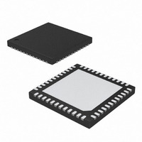
MAX17017GTM+ Maxim Integrated Products, MAX17017GTM+ Datasheet - Page 28

MAX17017GTM+
Manufacturer Part Number
MAX17017GTM+
Description
IC PWR SUPPLY CONTROLLER 48TQFN
Manufacturer
Maxim Integrated Products
Datasheet
1.MAX17017GTM.pdf
(31 pages)
Specifications of MAX17017GTM+
Applications
Power Supply Controller
Voltage - Input
5.5 ~ 28 V
Operating Temperature
-40°C ~ 105°C
Mounting Type
Surface Mount
Package / Case
48-TQFN Exposed Pad
Input Voltage
5.5 V to 24 V
Operating Temperature Range
- 40 C to + 105 C
Mounting Style
SMD/SMT
Duty Cycle (max)
300 uA
Supply Voltage Range
3V To 5V, 5.5V To 28V
Digital Ic Case Style
TQFN
No. Of Pins
48
Termination Type
SMD
No. Of Channels
4
Rohs Compliant
Yes
Filter Terminals
SMD
Leaded Process Compatible
Yes
Lead Free Status / RoHS Status
Lead free / RoHS Compliant
Current - Supply
-
Voltage - Supply
-
Lead Free Status / Rohs Status
Lead free / RoHS Compliant
Quad-Output Controller for
Low-Power Architecture
In general, if the ESR zero occurs before the Nyquist
pole, then canceling the ESR zero is recommended:
If:
then:
where R
divider.
The current in the boost converter input capacitor does
not contain large square-wave currents as found in the
output capacitor. Therefore, the input capacitor selec-
tion is less critical due to the output capacitor. However,
a low ESR is recommended.
The RMS input ripple current for a boost converter is:
The value of the IND bypass capacitor is chosen to limit
the amount of ripple and noise at IND, and the amount of
voltage sag during a load transient. Typically, IND con-
nects to the output of a step-down switching regulator,
which already has a large bulk output capacitor.
Nevertheless, a ceramic capacitor equivalent to half the
VTT output capacitance should be added and placed as
close as possible to IND. The necessary capacitance
value must be increased with larger load current, or if the
trace from IND to the power source is long and results in
relatively high input impedance.
The VTT output stage is powered from the IND input.
The VTT output voltage is set by the REFIND input.
REFIND sets the VTT LDO feedback regulation voltage
(V
VTT LDO (FBD voltage) and VTTR track the REFIND
voltage over a 0.5V to 1.5V range. This reference input
28
FBD
______________________________________________________________________________________
= V
FB
IND Input Capacitor Selection (C
REFIND
is the parallel impedance of the FB resistive
VTT LDO Design Procedure
I
CIN RMS
VTT LDO Output Voltage (FBD)
(
ESR
) and the VTTR output voltage. The
C
Step-Up Configuration Input
FB
)
>
≈
>
⎛
⎝ ⎜
(
⎛
⎜
⎝
0 3
1 -
C
.
G
OUT
CS OUT
V
D AV
R
IN MIN MAX
)
FB
Capacitor Selection
V
Lf
(
ESR
SW
REF
)
D
⎞
⎟
⎠
⎞
⎠ ⎟
IND
)
feature makes the MAX17017 ideal for memory applica-
tions in which the termination supply must track the
supply voltage.
A minimum value of 20μF or greater ceramic is needed
to stabilize the VTT output (OUTD). This value of capac-
itance limits the switching regulator’s unity-gain band-
width frequency to approximately 1.2MHz (typ) to allow
adequate phase margin for stability. To keep the
capacitor acting as a capacitor within the switching
regulator’s bandwidth, it is important that ceramic
capacitors with low ESR and ESL be used.
Since the gain bandwidth is also determined by the
transconductance of the output MOSFETs, which
increases with load current, the output capacitor might
need to be greater than 20μF if the load current
exceeds 1.5A, but can be smaller than 20μF if the maxi-
mum load current is less than 1.5A. As a guideline,
choose the minimum capacitance and maximum ESR
for the output capacitor using the following:
and:
R
frequency given by approximately:
Once these conditions for stability are met, additional
capacitors, including those of electrolytic and tantalum
types, can be connected in parallel to the ceramic
capacitor (if desired) to further suppress noise or volt-
age ripple at the output.
The VTTR buffer is a scaled-down version of the VTT
regulator, with much smaller output transconductance.
Therefore, the VTTR compensation requirements also
scale. For typical applications requiring load currents
up to ±3mA, a 0.22μF or greater ceramic capacitor is
recommended (R
ESR
value is measured at the unity-gain-bandwidth
VTTR Output Capacitor Selection
R
C
ESR MAX
OUT MIN
f
GBW
ESR
_
_
VTT LDO Output Capacitor
=
< 0.3Ω).
C
=
=
36
OUT
20
5
m
μF
Ω
×
×
×
Selection (C
I
LOAD
1 5 .
I
I
LOAD
1 5
LOAD
1 5
.
.
A
A
A
OUTD
)


