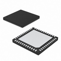
MAX17017GTM+ Maxim Integrated Products, MAX17017GTM+ Datasheet - Page 19

MAX17017GTM+
Manufacturer Part Number
MAX17017GTM+
Description
IC PWR SUPPLY CONTROLLER 48TQFN
Manufacturer
Maxim Integrated Products
Datasheet
1.MAX17017GTM.pdf
(31 pages)
Specifications of MAX17017GTM+
Applications
Power Supply Controller
Voltage - Input
5.5 ~ 28 V
Operating Temperature
-40°C ~ 105°C
Mounting Type
Surface Mount
Package / Case
48-TQFN Exposed Pad
Input Voltage
5.5 V to 24 V
Operating Temperature Range
- 40 C to + 105 C
Mounting Style
SMD/SMT
Duty Cycle (max)
300 uA
Supply Voltage Range
3V To 5V, 5.5V To 28V
Digital Ic Case Style
TQFN
No. Of Pins
48
Termination Type
SMD
No. Of Channels
4
Rohs Compliant
Yes
Filter Terminals
SMD
Leaded Process Compatible
Yes
Lead Free Status / RoHS Status
Lead free / RoHS Compliant
Current - Supply
-
Voltage - Supply
-
Lead Free Status / Rohs Status
Lead free / RoHS Compliant
When the bypass input (BYP) exceeds the LDO5 boot-
strap switchover threshold for more than 500μs, an
internal 1.5Ω (typ) p-channel MOSFET shorts BYP to
LDO5, while simultaneously disabling the LDO5 linear
regulator. This bootstraps the controller, allowing power
for the internal circuitry and external LDO5 loading to
be generated by the output of a 5V switching regulator.
Bootstrapping reduces power dissipation due to driver
and quiescent losses by providing power from a
switch-mode source, rather than from a much-less-effi-
cient linear regulator. The current capability increases
from 50mA to 100mA when the LDO5 output is
switched over to BYP. When BYP drops below the boot-
strap threshold, the controller immediately disables the
bootstrap switch and reenables the 5V LDO.
The 1.25V reference is accurate to ±1% over temperature
and load, making REF useful as a precision system refer-
ence. Bypass REF to GND with a 0.1μF or greater ceram-
ic capacitor. The reference sources up to 50μA and sinks
5μA to support external loads. If highly accurate specifi-
cations are required for the main SMPS output voltages,
the reference should not be loaded. Loading the refer-
ence slightly reduces the output voltage accuracy
because of the reference load-regulation error.
Figure 3. PWM Comparator Functional Diagram
SLOPE COMPENSATION
CSH_
CSL_
FB_
REF
______________________________________________________________________________________
I1
LDO5 Bootstrap Switchover
Reference (REF)
R1
I2
V
L
R2
Quad-Output Controller for
Low-Power Architecture
I3
The heart of each current-mode PWM controller is a
multi-input, open-loop comparator that sums multiple
signals: the output-voltage error signal with respect to
the reference voltage, the current-sense signal, and the
slope compensation ramp (Figure 3). The MAX17017
uses a direct-summing configuration, approaching
ideal cycle-to-cycle control over the output voltage
without a traditional error amplifier and the phase shift
associated with it.
The FREQ input selects the PWM mode switching fre-
quency. Table 1 shows the switching frequency based
on the FREQ connection. High-frequency (FREQ =
GND) operation optimizes the application for the small-
est component size, trading off efficiency due to higher
switching losses. This might be acceptable in ultra-
portable devices where the load currents are lower.
Low-frequency (FREQ = 5V) operation offers the best
overall efficiency at the expense of component size and
board space.
V
UNCOMPENSATED
HIGH-SPEED
LEVEL TRANSLATOR
AND BUFFER
SMPS Detailed Description
BIAS
Fixed-Frequency, Current-Mode
Frequency Selection (FREQ)
OUTPUT DRIVER
PWM Controller
TO PWM
LOGIC
19


