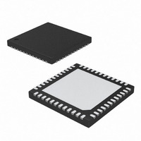
MAX17017GTM+ Maxim Integrated Products, MAX17017GTM+ Datasheet - Page 22

MAX17017GTM+
Manufacturer Part Number
MAX17017GTM+
Description
IC PWR SUPPLY CONTROLLER 48TQFN
Manufacturer
Maxim Integrated Products
Datasheet
1.MAX17017GTM.pdf
(31 pages)
Specifications of MAX17017GTM+
Applications
Power Supply Controller
Voltage - Input
5.5 ~ 28 V
Operating Temperature
-40°C ~ 105°C
Mounting Type
Surface Mount
Package / Case
48-TQFN Exposed Pad
Input Voltage
5.5 V to 24 V
Operating Temperature Range
- 40 C to + 105 C
Mounting Style
SMD/SMT
Duty Cycle (max)
300 uA
Supply Voltage Range
3V To 5V, 5.5V To 28V
Digital Ic Case Style
TQFN
No. Of Pins
48
Termination Type
SMD
No. Of Channels
4
Rohs Compliant
Yes
Filter Terminals
SMD
Leaded Process Compatible
Yes
Lead Free Status / RoHS Status
Lead free / RoHS Compliant
Current - Supply
-
Voltage - Supply
-
Lead Free Status / Rohs Status
Lead free / RoHS Compliant
Quad-Output Controller for
Low-Power Architecture
POKD is the open-drain output of a window comparator
that continuously monitors the VTT LDO output for
undervoltage and overvoltage conditions. POKD is
actively held low when the VTT LDO is disabled (OND
= GND) and soft-start. Once the startup blanking time
expires, POKD becomes high impedance as long as
the output remains within ±6% (min) of the nominal reg-
ulation voltage set by REFIND. POKD goes low once its
corresponding output drops or rises 12% (typ) beyond
its nominal regulation point or the output is shut down.
For a logic-level POKD output voltage, connect an
external pullup resistor between POKD and LDO5. A
100kΩ pullup resistor works well in most applications.
If the output voltage rises above 112% (typ) of its nomi-
nal regulation voltage, the controller sets the fault latch,
pulls POKD low, shuts down the source/sink linear reg-
ulator, and immediately pulls the output to ground
through its low-side MOSFET. Turning on the low-side
MOSFET with 100% duty cycle rapidly discharges the
output capacitors and clamps the output to ground.
Cycle V
latch and restart the linear regulator.
Each MAX17017 includes an output undervoltage pro-
tection (UVP) circuit that begins to monitor the output
once the startup blanking period has ended. If the
source/sink LDO output voltage drops below 88% (typ)
of its nominal REFIND regulation voltage for 5ms, the
UVP protection sets the fault latch, pulls the POKD out-
put low, forces the output into a high-impedance state,
and shuts down the linear regulator. Cycle V
1V or toggle OND to clear the fault latch and restart the
regulator.
Firmly establish the input voltage range and maximum
load current before choosing a switching frequency
and inductor operating point (ripple-current ratio). The
primary design trade-off lies in choosing a good switch-
ing frequency and inductor operating point, and the fol-
lowing four factors dictate the rest of the design:
• Input voltage range. The maximum value (V
22
must accommodate the worst-case, high AC-
adapter voltage. The minimum value (V
account for the lowest battery voltage after drops
______________________________________________________________________________________
VTT LDO Detailed Description
VTT LDO Power-Good Output (POKD)
CC
LDO Output Undervoltage Protection (UVP)
LDO Output Overvoltage Protection (OVP)
below 1V or toggle OND to clear the fault
SMPS Design Procedure
(Step Down Regulators)
VTT LDO Fault Protection
IN(MIN)
CC
IN(MAX)
) must
below
)
• Maximum load current. There are two values to
• Switching frequency. This choice determines the
• Inductor operating point. This choice provides
The switching frequency and inductor operating point
determine the inductor value as follows:
Find a low-loss inductor having the lowest possible DC
resistance that fits in the allotted dimensions. Most
inductor manufacturers provide inductors in standard
values, such as 1.0μH, 1.5μH, 2.2μH, 3.3μH, etc. Also
look for nonstandard values, which can provide a better
compromise in LIR across the input voltage range. If
using a swinging inductor (where the no-load induc-
tance decreases linearly with increasing current), evalu-
ate the LIR with properly scaled inductance values. For
due to connectors, fuses, and battery selector
switches. If there is a choice at all, lower input volt-
ages result in better efficiency.
consider. The peak load current (I
mines the instantaneous component stresses and fil-
tering requirements and thus drives output capacitor
selection, inductor saturation rating, and the design
of the current-limit circuit. The continuous load cur-
rent (I
thus drives the selection of input capacitors,
MOSFETs, and other critical heat-contributing com-
ponents.
basic trade-off between size and efficiency. The
optimal frequency is largely a function of maximum
input voltage, due to MOSFET switching losses that
are proportional to frequency and V
trade-offs between size vs. efficiency and transient
response vs. output ripple. Low inductor values pro-
vide better transient response and smaller physical
size, but also result in lower efficiency, higher output
ripple, and lower maximum load current, and due to
increased ripple currents. The minimum practical
inductor value is one that causes the circuit to oper-
ate at the edge of critical conduction (where the
inductor current just touches zero with every cycle at
maximum load). Inductor values lower than this
grant no further size-reduction benefit. The optimum
operating point is usually found between 20% and
50% ripple current. When pulse skipping (light
loads), the inductor value also determines the load-
current value at which PFM/PWM switchover occurs.
LOAD
) determines the thermal stresses and
L
=
Step-Down Inductor Selection
V f
IN SW LOAD MAX
V
OUT
I
(
V
IN
−
(
V
OUT
)
LIR
)
LOAD(MAX)
IN 2
.
) deter-


