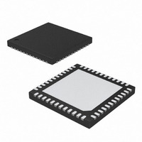
MAX17017GTM+ Maxim Integrated Products, MAX17017GTM+ Datasheet - Page 24

MAX17017GTM+
Manufacturer Part Number
MAX17017GTM+
Description
IC PWR SUPPLY CONTROLLER 48TQFN
Manufacturer
Maxim Integrated Products
Datasheet
1.MAX17017GTM.pdf
(31 pages)
Specifications of MAX17017GTM+
Applications
Power Supply Controller
Voltage - Input
5.5 ~ 28 V
Operating Temperature
-40°C ~ 105°C
Mounting Type
Surface Mount
Package / Case
48-TQFN Exposed Pad
Input Voltage
5.5 V to 24 V
Operating Temperature Range
- 40 C to + 105 C
Mounting Style
SMD/SMT
Duty Cycle (max)
300 uA
Supply Voltage Range
3V To 5V, 5.5V To 28V
Digital Ic Case Style
TQFN
No. Of Pins
48
Termination Type
SMD
No. Of Channels
4
Rohs Compliant
Yes
Filter Terminals
SMD
Leaded Process Compatible
Yes
Lead Free Status / RoHS Status
Lead free / RoHS Compliant
Current - Supply
-
Voltage - Supply
-
Lead Free Status / Rohs Status
Lead free / RoHS Compliant
Quad-Output Controller for
Low-Power Architecture
The load-transient response depends on the overall
output impedance over frequency, and the overall
amplitude and slew rate of the load step. In applica-
tions with large, fast load transients (load step > 80% of
full load and slew rate > 10A/μs), the output capacitor’s
high-frequency response—ESL and ESR—needs to be
considered. To prevent the output voltage from spiking
too low under a load-transient event, the ESR is limited
by the following equation (ignoring the sag due to finite
capacitance):
where V
the maximum load step, and R
resistance between the load and output capacitor.
The capacitance value dominates the midfrequency
output impedance and dominates the load-transient
response as long as the load transient’s slew rate is
less than two switching cycles. Under these conditions,
the sag and soar voltages depend on the output
capacitance, inductance value, and delays in the tran-
sient response. Low inductor values allow the inductor
current to slew faster, replenishing charge removed
from or added to the output filter capacitors by a sud-
den load step, especially with low differential voltages
across the inductor. The sag voltage (V
after applying the load current can be estimated by the
following:
where D
Electrical Characteristics table), T is the switching peri-
od (1/f
mode, or L x I
mode. The amount of overshoot voltage (V
occurs after load removal (due to stored inductor ener-
gy) can be calculated as:
When using low-capacity ceramic filter capacitors,
capacitor size is usually determined by the capacity
needed to prevent V
load transients. Generally, once enough capacitance is
added to meet the overshoot requirement, undershoot at
the rising load edge is no longer a problem.
24
V
SAG
______________________________________________________________________________________
OSC
=
STEP
2
MAX
C
), and ΔT equals V
OUT IN
R
is the allowed voltage drop, ΔI
L I
ESR
IDLE
(
V
is the maximum duty factor (see the
(
Δ
SOAR
V
LOAD MAX
Internal SMPS Transient Response
/(V
≤
×
SOAR
⎛
⎜
⎝
D
IN
≈
(
Δ
MAX
I
LOAD MAX
(
- V
Δ
V
2
I
from causing problems during
)
LOAD MAX
STEP
−
OUT
)
C
2
V
OUT OUT
(
OUT
OUT
PCB
) when in pulse-skipping
(
V
)
/V
)
+
is the parasitic board
−
IN
Δ
)
R
)
I
PCB
LOAD MAX
2
x T when in PWM
L
SAG
⎞
⎟
⎠
C
(
LOAD(MAX)
) that occurs
OUT
SOAR
)
(
T
−
) that
Δ
T
)
is
The input capacitor must meet the ripple current
requirement (I
The I
determined by the following equation:
The worst-case RMS current requirement occurs when
operating with V
equation simplifies to I
MAX17017 uses an interleaved fixed-frequency archi-
tecture, which helps reduce the overall input RMS cur-
rent on the INBC input supply.
For the MAX17017 system (INA) supply, nontantalum
chemistries (ceramic, aluminum, or OS-CON) are pre-
ferred due to their resistance to inrush surge currents
typical of systems with a mechanical switch or connector
in series with the input. For the MAX17017 INBC input
supply, ceramic capacitors are preferred on input due to
their low parasitic inductance, which helps reduce the
high-frequency ringing on the INBC supply when the
internal MOSFETs are turned off. Choose an input
capacitor that exhibits less than +10°C temperature rise
at the RMS input current for optimal circuit longevity.
The boost capacitors (C
enough to handle the gate charging requirements of
the high-side MOSFETs. For these low-power applica-
tions, 0.1μF ceramic capacitors work well.
Most of the following MOSFET guidelines focus on the
challenge of obtaining high load-current capability
when using high-voltage (> 20V) AC adapters. Low-
current applications usually require less attention.
The high-side MOSFET (N
the resistive losses plus the switching losses at both
V
should be roughly equal to the losses at V
lower losses in between. If the losses at V
significantly higher, consider increasing the size of N
Conversely, if the losses at V
higher, consider reducing the size of N
not vary over a wide range, maximum efficiency is
achieved by selecting a high-side MOSFET (N
has conduction losses equal to the switching losses.
Choose a low-side MOSFET (N
possible on-resistance (R
ate-sized package (i.e., 8-pin SO, DPAK, or D
IN(MIN)
RMS
Regulator A Power-MOSFET Selection
and V
requirements of an individual regulator can be
I
RMS
RMS
IN(MAX)
=
IN
⎛
⎜
⎝
) imposed by the switching currents.
I
LOAD
= 2V
V
IN
Input Capacitor Selection
RMS
. Ideally, the losses at V
⎞
⎟
⎠
OUT
BST
DS(ON)
H
= 0.5 x I
V
) must be able to dissipate
OUT IN
. At this point, the above
) must be selected large
IN(MAX)
(
L
), comes in a moder-
V
) that has the lowest
BST Capacitors
LOAD.
−
V
are significantly
OUT
H
However, the
. If V
IN(MAX)
)
IN(MIN)
IN
IN(MIN)
H
2
PAK),
) that
, with
does
are
H
.


