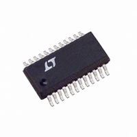
LTC1702IGN#TR Linear Technology, LTC1702IGN#TR Datasheet - Page 11

LTC1702IGN#TR
Manufacturer Part Number
LTC1702IGN#TR
Description
IC REG SW DUAL SYNC 2PH 24SSOP
Manufacturer
Linear Technology
Series
PolyPhase®r
Type
Step-Down (Buck)r
Datasheet
1.LTC1702CGN.pdf
(36 pages)
Specifications of LTC1702IGN#TR
Internal Switch(s)
No
Synchronous Rectifier
Yes
Number Of Outputs
2
Current - Output
1A, 25A
Frequency - Switching
550kHz
Voltage - Input
3 ~ 7 V
Operating Temperature
-40°C ~ 85°C
Mounting Type
Surface Mount
Package / Case
24-SSOP
Lead Free Status / RoHS Status
Contains lead / RoHS non-compliant
Voltage - Output
-
Power - Output
-
Available stocks
Company
Part Number
Manufacturer
Quantity
Price
APPLICATIONS
improves loop phase margin (see Figure 3). The Feedback
Loop/Compensation section contains a detailed explana-
tion of type 3 feedback loops.
MIN/MAX
Two additional feedback loops keep an eye on the primary
feedback amplifier and step in if the feedback node moves
±5% from its nominal 800mV value. The MAX comparator
(see Block Diagram) activates whenever FB rises more
than 5% above 800mV. It immediately turns the top
MOSFET (QT) off and the bottom MOSFET (QB) on and
keeps them that way until FB falls back within 5%. This
pulls the output down as fast as possible, preventing
damage to the (often expensive) load. If FB rises because
the output is shorted to a higher supply, QB will stay on
until the short goes away, the higher supply current limits
or QB dies trying to save the load. This behavior provides
maximum protection against overvoltage faults at the
output, while allowing the circuit to resume normal opera-
tion when the fault is removed. The overvoltage protection
circuit can optionally be set to latch the output off perma-
nently (see the Overvoltage Fault section).
The MIN comparator (see Block Diagram) trips whenever
FB is more than 5% below 800mV and immediately forces
the switch duty cycle to 90% to bring the output voltage
back into range. It releases when FB is within the 5%
window. MIN is disabled when the soft-start or current
limit circuits are active—the only two times that the
output should legitimately be below its regulated value.
COMP
R2
Figure 3. “Type 3” Feedback Loop
FB
C2
U
+
–
INFORMATION
0.8V
C1
U
FB
W
R
B
R3
R1
C3
U
V
1702 F03
OUT
Notice that the FB pin is the virtual ground node of the
feedback amplifier. A typical compensation network does
not include local DC feedback around the amplifier, so that
the DC level at FB will be an accurate replica of the output
voltage, divided down by R1 and R
the compensation capacitors will tend to attenuate AC
signals at FB, especially with low bandwidth type 1 feed-
back loops. This creates a situation where the MIN and
MAX comparators do not respond immediately to shifts in
the output voltage, since they monitor the output at FB.
Maximizing feedback loop bandwidth will minimize these
delays and allow MIN and MAX to operate properly. See
the Feedback Loop/Compensation section.
PGOOD Flags
The MIN comparator performs another function; it drives
the external “power good” pin (PGOOD) through a 100µs
delay stage. PGOOD is an open-drain output, allowing it to
be wire-OR’ed with other open-drain/open-collector sig-
nals. An external pull-up resistor is required for PGOOD to
swing high. Any time the FB pin is more than 5% below the
programmed value for more than 100µs, PGOOD will pull
low, indicating that the output is out of regulation. PGOOD
remains active during soft-start and current limit, even
though the MIN comparator has no effect on the duty cycle
during these times. The 100µs delay ensures that short
output transient glitches that are successfully “caught” by
the MIN comparator don’t cause momentary glitches at
the PGOOD pin. Note that the PGOOD pin only watches
MIN, not MAX—it does not indicate if the output is 5%
above the programmed value.
When either side of the LTC1702 is in shutdown, its
associated PGOOD pin will go high. This behavior allows
a valid PGOOD reading when the two PGOOD pins are tied
together, even if one side is shut down. It also reduces
quiescent current by eliminating the excess current drawn
by the pull-up at the PGOOD pin. As soon as the RUN/SS
pin rises above the shutdown threshold and the side
comes out of shutdown, the PGOOD pin will pull low until
the output voltage is valid. If both sides are shut down at
the same time, both PGOOD pins will go high. To avoid
confusion, if either side of the LTC1702 is shut down, the
host system should ignore the associated PGOOD pin.
B
(Figure 3). However,
LTC1702
11
1702fa


