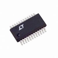
LTC1702IGN#TR Linear Technology, LTC1702IGN#TR Datasheet - Page 26

LTC1702IGN#TR
Manufacturer Part Number
LTC1702IGN#TR
Description
IC REG SW DUAL SYNC 2PH 24SSOP
Manufacturer
Linear Technology
Series
PolyPhase®r
Type
Step-Down (Buck)r
Datasheet
1.LTC1702CGN.pdf
(36 pages)
Specifications of LTC1702IGN#TR
Internal Switch(s)
No
Synchronous Rectifier
Yes
Number Of Outputs
2
Current - Output
1A, 25A
Frequency - Switching
550kHz
Voltage - Input
3 ~ 7 V
Operating Temperature
-40°C ~ 85°C
Mounting Type
Surface Mount
Package / Case
24-SSOP
Lead Free Status / RoHS Status
Contains lead / RoHS non-compliant
Voltage - Output
-
Power - Output
-
Available stocks
Company
Part Number
Manufacturer
Quantity
Price
APPLICATIONS
LTC1702
to an intermediate supply voltage, often 5V. The LTC1702
then converts the intermediate voltage to the low voltage,
high current supplies required by the system. Compared
to a 1-step converter that converts a high input voltage
directly to a very low output voltage, the 2-step converter
exhibits superior transient response, smaller component
size and equivalent efficiency. Thermal management and
layout complexity are also improved with a 2-step
approach.
A typical notebook computer supply might use a 4-cell
Li-Ion battery pack as an input supply with a 15V nominal
terminal voltage. The logic circuits require 5V/3A and 3.3V/
5A to power system board logic, and 2.5V/0.5A, 1.8V/2A
and 1.5V/10A to power the CPU. A typical 2-step conver-
sion system would use a step-down switcher (perhaps an
LTC1628 or two LTC1625s) to convert 15V to 5V and
another to convert 15V to 3.3V (Figure 14). One channel of
the LTC1702 would generate the 1.5V supply using the
3.3V supply as the input and the other channel would gen-
erate 1.8V using the 5V supply as the input. The corre-
sponding 1-step system would use four similar step-down
switchers, each using 15V as the input supply and gener-
ating one of the four output voltages. Since the 2.5V sup-
ply represents a small fraction of the total output power,
either system can generate it from the 3.3V output using
an LDO linear regulator, without the 75% linear efficiency
making much of an impact on total system efficiency.
26
V
15V
Figure 14. 2-Step Conversion Block Diagram
BAT
*OR TWO LTC1625s
LTC1628*
U
INFORMATION
U
LTC1702
LDO
W
5V/3A
1.8V/2A
1.5V/10A
3.3V/5A
2.5V/0.5A
1702 F14
U
Clearly, the 5V and 3.3V sections of the two schemes are
equivalent. The 2-step system draws additional power
from the 5V and 3.3V outputs, but the regulation tech-
niques and trade-offs at these outputs are similar. The
difference lies in the way the 1.8V and 1.5V supplies are
generated. For example, the 2-step system converts 3.3V
to 1.5V with a 45% duty cycle. During the QT on-time, the
voltage across the inductor is 1.8V and during the QB
on-time, the voltage is 1.5V, giving roughly symmetrical
transient response to positive and negative load steps. The
1.8V maximum voltage across the inductor allows the use
of a small 0.47µH inductor while keeping ripple current
under 4A (40% of the 10A maximum load). By contrast,
the 1-step converter is converting 15V to 1.5V, requiring
just a 10% duty cycle. Inductor voltages are now 13.5V
when QT is on and 1.5V when QB is on, giving vastly
different di/dt values and correspondingly skewed tran-
sient response with positive and negative current steps.
The narrow 10% duty cycle usually requires a lower
switching frequency, which in turn requires a higher value
inductor and larger output capacitor. Parasitic losses due
to the large voltage swing at the source of QT cost
efficiency, eliminating any advantage the 1-step conver-
sion might have had.
Note that power dissipation in the LTC1702 portion of a
2-step circuit is lower than it would be in a typical 1-step
converter, even in cases where the 1-step converter has
higher total efficiency than the 2-step system. In a typical
microprocessor core supply regulator, for example, the
regulator is usually located right next to the CPU. In a
1-step design, all of the power dissipated by the core
regulator is right there next to the hot CPU, aggravating
thermal management. In a 2-step LTC1702 design, a
significant percentage of the power lost in the core regu-
lation system happens in the 5V or 3.3V supply, which is
usually away from the CPU. The power lost to heat in the
LTC1702 section of the system is relatively low, minimiz-
ing the heat near the CPU.
1702fa


