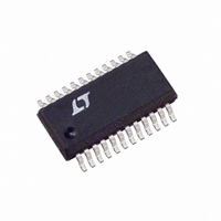
LTC1702IGN#TR Linear Technology, LTC1702IGN#TR Datasheet - Page 6

LTC1702IGN#TR
Manufacturer Part Number
LTC1702IGN#TR
Description
IC REG SW DUAL SYNC 2PH 24SSOP
Manufacturer
Linear Technology
Series
PolyPhase®r
Type
Step-Down (Buck)r
Datasheet
1.LTC1702CGN.pdf
(36 pages)
Specifications of LTC1702IGN#TR
Internal Switch(s)
No
Synchronous Rectifier
Yes
Number Of Outputs
2
Current - Output
1A, 25A
Frequency - Switching
550kHz
Voltage - Input
3 ~ 7 V
Operating Temperature
-40°C ~ 85°C
Mounting Type
Surface Mount
Package / Case
24-SSOP
Lead Free Status / RoHS Status
Contains lead / RoHS non-compliant
Voltage - Output
-
Power - Output
-
Available stocks
Company
Part Number
Manufacturer
Quantity
Price
BLOCK
LTC1702
PIN
FB2 (Pin 14): Controller 2 Feedback Input. See FB1.
COMP2 (Pin 15): Controller 2 Loop Compensation. See
COMP1.
RUN/SS2 (Pin 16): Controller 2 Run/Soft-start. See RUN/
SS1.
FAULT (Pin 17): Output Overvoltage Fault (Latched). The
FAULT pin is an open-drain output with an internal 10µA
pull-up. If either regulated output voltage rises more than
15% above its programmed value for more than 25µs, the
FAULT output will go high and the entire LTC1702 will be
disabled. When FAULT is high, both BG pins will go high,
turning on the bottom MOSFET switches and pulling down
the high output voltage. The LTC1702 will remain latched
in this state until the power is cycled. When FAULT mode
is active, the FAULT pin will be pulled up with an internal
10µA current source. Tying FAULT directly to PGND will
6
U
FUNCTIONS
RUN/SS1,2
COMP1,2
I
U
MAX1,2
DIAGRAM
10µA
V
CC
550mV
U
550kHz
OSC
3.5µA
W
I
LIM
THIS CONTROLLER
SHUTDOWN TO
800mV
1V
90% DUTY CYCLE
START
+
SOFT
P-P
FB
CONTROLLER
–
OTHER
FROM
760mV
MIN
840mV
MAX
SHUTDOWN TO
ENTIRE CHIP
BURST
LOGIC
disable latched FAULT mode and will allow the LTC1702 to
resume normal operation when the overvoltage fault is
removed.
PGOOD2 (Pin 18): Controller 2 Power Good. See PGOOD1.
PGND (Pin 19): Power Ground. The BG n drivers return to
this pin. Connect PGND to a high current ground node in
close proximity to the sources of external MOSFETs, QB1
and QB2, and the V
SW2 (Pin 20): Controller 2 Switching Node. See SW1.
TG2 (Pin 21): Controller 2 Top Gate Drive. See TG1.
BG2 (Pin 22): Controller 2 Bottom Gate Drive. See BG1.
BOOST2 (Pin 23): Controller 2 Top Gate Driver Supply.
See BOOST1.
I
MAX2
920mV
FLT
(Pin 24): Controller 2 Current Limit Set. See I
FCB
DELAY
DELAY
100µs
25µs
DRIVE
LOGIC
CONTROLLER
OTHER
FROM
IN
and V
PV
DIS
CC
OUT
bypass capacitors.
BOOST1,2
TG1,2
SW1,2
BG1,2
PGND
SGND
PGOOD1,2
FAULT
FB1,2
1702 BD
MAX1
1702fa
.


