LTC1702IGN#TR Linear Technology, LTC1702IGN#TR Datasheet - Page 29

LTC1702IGN#TR
Manufacturer Part Number
LTC1702IGN#TR
Description
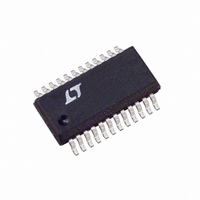
IC REG SW DUAL SYNC 2PH 24SSOP
Manufacturer
Linear Technology
Series
PolyPhase®r
Type
Step-Down (Buck)r
Datasheet
1.LTC1702CGN.pdf
(36 pages)
Specifications of LTC1702IGN#TR
Internal Switch(s)
No
Synchronous Rectifier
Yes
Number Of Outputs
2
Current - Output
1A, 25A
Frequency - Switching
550kHz
Voltage - Input
3 ~ 7 V
Operating Temperature
-40°C ~ 85°C
Mounting Type
Surface Mount
Package / Case
24-SSOP
Lead Free Status / RoHS Status
Contains lead / RoHS non-compliant
Voltage - Output
-
Power - Output
-
Available stocks
Company
Part Number
Manufacturer
Quantity
Price
APPLICATIONS
cycles. Over just a few cycles, however, the external
components conspire to limit the speed that the output
can move. Consider our typical 5V to 1.6V circuit, sub-
jected to a 1A to 5A load transient. Initially, the loop is in
regulation and the DC current in the output capacitor is
zero. Suddenly, an extra 4A start flowing out of the output
capacitor while the inductor is still supplying only 1A. This
sudden change will generate a (4A)(C
the output; with a typical 0.015Ω output capacitor ESR,
this is a 60mV step at the output, or 3.8% (for a 1.6V output
voltage).
Very quickly, the feedback loop will realize that something
has changed and will move at the bandwidth allowed by
the external compensation network towards a new duty
cycle. If the bandwidth is set to 50kHz, the COMP pin will
get to 60% of the way to 90% duty cycle in 3µs. Now the
inductor is seeing 3.5V across itself for a large portion of
the cycle, and its current will increase from 1A at a rate set
by di/dt = V/L. If the inductor value is 0.5µH, the di/dt will
be 3.5V/0.5µH or 7A/µs. Sometime in the next few micro-
seconds after the switch cycle begins, the inductor current
will have risen to the 5A level of the load current and the
output capacitor will stop losing charge.
V
SW
Figure 16a. Capacitor Parasitics
Affecting Transient Recovery
C
I
L
OUT
L
+
–
+
–
V
V
ESR
CAP
U
INFORMATION
U
1702 F16a
I
OUT
V
OUT
W
ESR
)voltage step at
V
V
V
I
OUT
OUT
ESR
CAP
I
L
U
Note that the output voltage will stop dropping before the
inductor current reaches this new output current level.
Recall that any practical output capacitor looks like a pure
capacitance in series with some amount of ESR. When a
load transient hits, virtually all of the initial voltage drop at
the output is due to IR drop across the ESR. The output
capacitance begins to discharge at the same time and
continues until the inductor current rises to match the new
output current level.
The output voltage, however, will turn around and start
heading the right way before this happens. The next time
the top MOSFET turns on, the inductor current will begin
increasing linearly. This increasing current flows almost
entirely into the capacitor, going through the ESR as it
does so (Figure 16). Positive di/dt in the inductor causes
positive dv/dt in the ESR, regardless of what the “pure”
capacitance is doing. The output voltage will turn around
when the positive dv/dt across the ESR exceeds the
negative dv/dt across the pure capacitance. If the expected
load step (∆I) is known, an optimum inductor value can be
chosen:
TRANSIENT
HITS
L
Figure 16b. Transient Recovery Curves
≤
AROUND
TURNS
V
(
OUT
V
IN
–
V
OUT
I
L
)
> I
• •
OUT
C
ESR
∆
I
TIME
V
OUT(NOMINAL)
V
V
V
I
OUT
ESR
CAP
OUT
I
L
LTC1702
29
1702 F16b
1702fa


