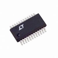
LTC1702IGN#TR Linear Technology, LTC1702IGN#TR Datasheet - Page 21

LTC1702IGN#TR
Manufacturer Part Number
LTC1702IGN#TR
Description
IC REG SW DUAL SYNC 2PH 24SSOP
Manufacturer
Linear Technology
Series
PolyPhase®r
Type
Step-Down (Buck)r
Datasheet
1.LTC1702CGN.pdf
(36 pages)
Specifications of LTC1702IGN#TR
Internal Switch(s)
No
Synchronous Rectifier
Yes
Number Of Outputs
2
Current - Output
1A, 25A
Frequency - Switching
550kHz
Voltage - Input
3 ~ 7 V
Operating Temperature
-40°C ~ 85°C
Mounting Type
Surface Mount
Package / Case
24-SSOP
Lead Free Status / RoHS Status
Contains lead / RoHS non-compliant
Voltage - Output
-
Power - Output
-
Available stocks
Company
Part Number
Manufacturer
Quantity
Price
APPLICATIONS
feedback amplifier, on the other hand, gives us a handle
with which to adjust the AC response. The goal is to have
180° phase shift at DC (so the loop regulates) and some-
thing less than 360° phase shift at the point that the loop
gain falls to 0dB. The simplest strategy is to set up the
feedback amplifier as an inverting integrator, with the 0dB
frequency lower than the LC pole (Figure 9). This “type 1”
GAIN
GAIN
(dB)
(dB)
Figure 9a. Type 1 Amplifier Schematic Diagram
A
Figure 8. Transfer Function of Buck Modulator
Figure 9b. Type 1 Amplifier Transfer Function
0
0
V
IN
GAIN
PHASE
R1
PHASE
U
R
B
GAIN
V
–12dB/OCT
INFORMATION
REF
U
+
–
C1
–6dB/OCT
W
–6dB/OCT
1702 F09a
OUT
1702 F08
PHASE
1702 F09b
0
–90
–180
(DEG)
0
–90
–180
–270
PHASE
(DEG)
U
configuration is stable but transient response will be less
than exceptional if the LC pole is at a low frequency.
Figure 10 shows an improved “type 2” circuit that uses an
additional pole-zero pair to temporarily remove 90° of
phase shift. This allows the loop to remain stable with 90°
more phase shift in the LC section, provided the loop
reaches 0dB gain near the center of the phase “bump.”
Type 2 loops work well in systems where the ESR zero in
the LC roll-off happens close to the LC pole, limiting the
total phase shift due to the LC. The additional phase
compensation in the feedback amplifier allows the 0dB
point to be at or above the LC pole frequency, improving
loop bandwidth substantially over a simple type 1 loop. It
has limited ability to compensate for LC combinations
where low capacitor ESR keeps the phase shift near 180°
for an extended frequency range. LTC1702 circuits using
conventional switching grade electrolytic output capaci-
tors can often get acceptable phase margin with type 2
compensation.
GAIN
(dB)
Figure 10a. Type 2 Amplifier Schematic Diagram
Figure 10b. Type 2 Amplifier Transfer Function
0
IN
GAIN
PHASE
R1
–6dB/OCT
R
B
V
REF
R2
+
–
C2
–6dB/OCT
C1
1702 F10a
LTC1702
OUT
PHASE
0
–90
–180
–270
(DEG)
1702 F10b
21
1702fa


