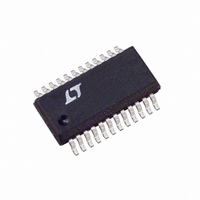
LTC1702IGN#TR Linear Technology, LTC1702IGN#TR Datasheet - Page 16

LTC1702IGN#TR
Manufacturer Part Number
LTC1702IGN#TR
Description
IC REG SW DUAL SYNC 2PH 24SSOP
Manufacturer
Linear Technology
Series
PolyPhase®r
Type
Step-Down (Buck)r
Datasheet
1.LTC1702CGN.pdf
(36 pages)
Specifications of LTC1702IGN#TR
Internal Switch(s)
No
Synchronous Rectifier
Yes
Number Of Outputs
2
Current - Output
1A, 25A
Frequency - Switching
550kHz
Voltage - Input
3 ~ 7 V
Operating Temperature
-40°C ~ 85°C
Mounting Type
Surface Mount
Package / Case
24-SSOP
Lead Free Status / RoHS Status
Contains lead / RoHS non-compliant
Voltage - Output
-
Power - Output
-
Available stocks
Company
Part Number
Manufacturer
Quantity
Price
LTC1702
APPLICATIONS
below ground. If latched FAULT mode is used, a Schottky
diode should be added with its cathode at the output and
its anode at ground to clamp the negative voltage to a safe
level and prevent possible damage to the load and the
output capacitors.
Note that in overvoltage conditions, the MAX comparator
will kick in at just +5%, turning QB on continuously long
before the output reaches +15%. Under most fault condi-
tions, this is adequate to bring the output back down
without firing the fault latch. Additionally, if MAX success-
fully keeps the output below +15%, the LTC1702 will
resume normal regulation as soon as the output overvolt-
age fault is resolved.
In some circuits, the OV latch can be a liability. Consider
a circuit where the output voltage at one channel may be
changed on the fly by switching in different feedback
resistors. A downward adjustment of greater than 15%
will fire the fault latch, disabling both sides of the LTC1702
until the power is recycled. In circuits such as this, the fault
latch can be disabled by grounding the FAULT pin. The
internal latch will still be set the first time the output
exceeds +15%, but the 10µA current source pull-up will
not be able to pull FAULT high, and the LTC1702 will ignore
the latch and continue normal operation. The MAX com-
parator will act as usual, turning on QB until output is
within range and then allowing the loop to resume normal
operation. FAULT can also be pulled down with external
open-collector logic to restart a fault-latched LTC1702 as
an alternative to recycling the power. Note that this will not
reset the internal latch; if the external pull-down is
released, the LTC1702 will reenter FAULT mode. To reset
the latch, pull both RUN/SS pins low simultaneously or
cycle the input power.
EXTERNAL COMPONENT SELECTION
POWER MOSFETs
Getting peak efficiency out of the LTC1702 depends strongly
on the external MOSFETs used. The LTC1702 requires at
least two external MOSFETs per side—more if one or
more of the MOSFETs are paralleled to lower on-resis-
tance. To work efficiently, these MOSFETs must exhibit
16
U
INFORMATION
U
W
U
low R
is 3.3V) to minimize resistive power loss while they are
conducting current. They must also have low gate charge
to minimize transition losses during switching. On the
other hand, voltage breakdown requirements in a typical
LTC1702 circuit are pretty tame: the 7V maximum input
voltage limits the V
safe levels for most devices.
Low R
R
the resistance from the drain to the source of the MOSFET
when the gate is fully on. Many MOSFETs have R
specified at 4.5V gate drive—this is the right number to
use in LTC1702 circuits running from a 5V supply. As
current flows through this resistance while the MOSFET is
on, it generates I
flowing (usually equal to the output current) and R is the
MOSFET R
MOSFET is on. When it is off, the current is zero and the
power lost is also zero (and the other MOSFET is busy
losing power).
This lost power does two things: it subtracts from the
power available at the output, costing efficiency, and it
makes the MOSFET hotter—both bad things. The effect is
worst at maximum load when the current in the MOSFETs
and thus the power lost are at a maximum. Lowering
R
additional gate charge (usually) and more cost (usually).
Proper choice of MOSFET R
between tolerable efficiency loss, power dissipation and
cost. Note that while the lost power has a significant effect
on system efficiency, it only adds up to a watt or two in a
typical LTC1702 circuit, allowing the use of small, surface
mount MOSFETs without heat sinks.
Gate Charge
Gate charge is amount of charge (essentially, the number
of electrons) that the LTC1702 needs to put into the gate
of an external MOSFET to turn it on. The easiest way to
visualize gate charge is to think of it as a capacitance from
the gate pin of the MOSFET to SW (for QT) or to PGND (for
DS(ON)
DS(ON)
DS(ON)
DS(ON)
calculations are pretty straightforward. R
improves heavy load efficiency at the expense of
DS(ON)
at 5V V
2
. This heat is only generated when the
R watts of heat, where I is the current
GS
DS
(3.3V V
and V
GS
DS(ON)
GS
the MOSFETs can see to
if the PV
becomes a trade-off
CC
input supply
DS(ON)
DS(ON)
1702fa
is


