LTC1702IGN#TR Linear Technology, LTC1702IGN#TR Datasheet - Page 24

LTC1702IGN#TR
Manufacturer Part Number
LTC1702IGN#TR
Description
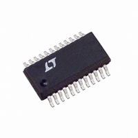
IC REG SW DUAL SYNC 2PH 24SSOP
Manufacturer
Linear Technology
Series
PolyPhase®r
Type
Step-Down (Buck)r
Datasheet
1.LTC1702CGN.pdf
(36 pages)
Specifications of LTC1702IGN#TR
Internal Switch(s)
No
Synchronous Rectifier
Yes
Number Of Outputs
2
Current - Output
1A, 25A
Frequency - Switching
550kHz
Voltage - Input
3 ~ 7 V
Operating Temperature
-40°C ~ 85°C
Mounting Type
Surface Mount
Package / Case
24-SSOP
Lead Free Status / RoHS Status
Contains lead / RoHS non-compliant
Voltage - Output
-
Power - Output
-
Available stocks
Company
Part Number
Manufacturer
Quantity
Price
APPLICATIONS
LTC1702
CURRENT LIMIT PROGRAMMING
Programming the current limit on the LTC1702 is straight-
forward. The I
maximum allowable voltage drop across QB (the bottom
MOSFET) before the current limit circuit engages. The
voltage across QB is set by its on-resistance and the
current flowing in the inductor, which is the same as the
output current. The LTC1702 current limit circuit inverts
the voltage at I
voltage across QB, allowing the current limit to be set with
a positive voltage.
To set the current limit, calculate the expected voltage drop
across QB at the maximum desired current:
I
expected operating current, to allow for MOSFET R
changes with temperature. Setting I
maximum normal operating current is usually safe and will
adequately protect the power components if they are
chosen properly. The CF term is an approximate factor that
corrects for errors caused by ringing on the switch node
(illustrated in Figure 6). This correction factor will change
depending on the layout and the components used, but
100mV is usually a good starting point. To provide ad-
equate margin and to accommodate for offsets and exter-
nal variations, it is recommended that V
with CF = 100 ± 50mV.
V
internal 10µA pull-up and an external resistor:
The resulting value of R
circuit to ensure that the I
MOSFET R
automobiles, and should be taken with a grain of salt.
Circuits that use very low values for R
be checked carefully, since small changes in R
cause large I
factor makes up a large percentage of the total V
value. If V
start up.
24
LIM
PROG
R
V
ILIM
PROG
should be chosen to be quite a bit higher than the
is then programmed at the I
= V
=
PROG
DS(ON)
(
PROG
I
ILIM
LIM
MAX
MAX
is set too low, the LTC1702 may fail to
/10µA
)
(
changes when the 100mV correction
pin sets the current limit by setting the
specs are like horsepower ratings in
R
U
before comparing it with the negative
DS ON
ILIM
(
INFORMATION
LIM
U
)
)
should be checked in an actual
+
circuit kicks in as expected.
CF
W
LIM
IMAX
MAX
PROG
to 150% of the
(< 20k) should
pin using the
be calculated
U
IMAX
DS(ON)
PROG
can
Accuracy Trade-Offs
The V
particularly accurate, primarily due to uncertainty in the
R
arises from the ringing present at the SW pin, which
causes the V
beginning of QB’s on-time. These inaccuracies do not
prevent the LTC1702 current limit circuit from protecting
itself and the load from damaging overcurrent conditions,
but they do prevent the user from setting the current limit
to a tight tolerance if more than one copy of the circuit is
being built. The 50% factor in the current setting equation
above reflects the margin necessary to ensure that the
circuit will stay out of current limit at the maximum normal
load, even with a hot MOSFET that is running quite a bit
higher than its R
FCB OPERATION/SECONDARY WINDINGS
The FCB pin can be used in conjunction with a secondary
winding on one side of the LTC1702 to generate a third
regulated voltage output. This output can be directly
regulated at the FCB pin. In theory, a fourth output could
be added, either unregulated or with additional external
circuitry at the FCB pin.
The extra auxiliary output is taken from a second winding
on the core of the inductor on one channel, converting it
into a transformer (Figure 13). The auxiliary output voltage
is set by the main output voltage and the turns ratio of the
extra winding to the primary winding. Load regulation at
the auxiliary output will be relatively good as long as the
main output is running in continuous mode. As the load on
the main channel drops and the LTC1702 switches to
discontinuous or Burst Mode operation, the auxiliary
output will not be able to maintain regulation, especially if
the load at the auxiliary output remains heavy.
To avoid this, the auxiliary output voltage can be divided
down with a conventional feedback resistor string with the
divided auxiliary output voltage fed back to the FCB pin
(Figure 13). The FCB pin threshold is trimmed to 800mV
DS(ON)
DS
from MOSFET to MOSFET. A second error term
sensing scheme used in the LTC1702 is not
DS
to look larger than (I
DS(ON)
spec.
LOAD
)(R
DS(ON)
) at the
1702fa


